用于超薄柔性微电子器件的超快激光诱导限厚烧结金属纳米粒子薄膜
IF 8.2
2区 材料科学
Q1 MATERIALS SCIENCE, MULTIDISCIPLINARY
引用次数: 0
摘要
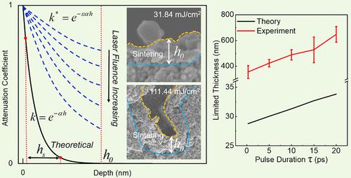
激光烧结金属纳米粒子(NPs)已广泛应用于柔性微电子器件的制造,其中烧结层厚度是影响机械稳定性和导电性的关键因素。在这项工作中,通过超快激光诱导金属 NP 薄膜的限厚烧结,在柔性基底上制造出了具有牢固结合力和优异导电性的超薄柔性电子电路。当激光通量低于金属 NP 膜的损伤阈值时,烧结层厚度可由激光参数控制。在激光脉冲持续时间为 0.3、5、10、15 和 20 ps 时,致密烧结 NP 层的最大厚度分别限制在 355、421、491、527 和 647 nm。这种厚度受限的烧结层主要是由金属 NP 的等离子体光热吸收和 NP 层内的热传导决定的。由于在强超快激光照射下的非热处理过程,金属与聚合物之间的相互作用可以进一步增强,而对基底的破坏却微乎其微。在脉冲持续时间为 20 ps 的激光烧结过程中,接收到的 Ag NP 薄膜的电阻率降至 6.32 μΩ-cm。同时,在经过 105 次弯曲循环、500 次胶带剥离循环和 60 分钟的水流冲击后,NP 薄膜的相对电阻分别增加到 2.7、1.7 和 1.03。这种利用超快激光烧结技术制备的厚度可控超薄银氧化物薄膜具有优异的机械坚固性和导电性,在超薄柔性微电子器件中大有可为。本文章由计算机程序翻译,如有差异,请以英文原文为准。
Ultrafast Laser-Induced Thickness-Limited Sintering of Metal Nanoparticle Film for Ultrathin Flexible Microelectronic Devices
Laser sintering of metal nanoparticles (NPs) has been widely used in flexible microelectronic device fabrication, wherein the sintered layer thickness is a key factor affecting the mechanical stability and conductivity. In this work, ultrathin flexible electronic circuits on flexible substrates with robust bonds and excellent conductivity have been fabricated through ultrafast laser-induced thickness-limited sintering of the metal NP film. When the laser fluence is below the damage threshold of the metal NP film, sintered layer thickness can be controlled by the laser parameters. The maximum thickness of the dense sintered NP layer is limited to 355, 421, 491, 527, and 647 nm at laser pulse durations of 0.3, 5, 10, 15, and 20 ps, respectively. This thickness-limited sintered layer is mainly determined by the plasmonic photothermal absorption of metal NPs and heat transfer within the NP layer. Due to the nonthermal process under intense ultrafast laser irradiation, the metal–polymer interaction can be further enhanced with minimal damage on substrates. The resistivity of the as-received Ag NP film decreases to 6.32 μΩ·cm after laser sintering at a pulse duration of 20 ps. Meanwhile, the relative resistance of the NP film increases to 2.7, 1.7, and 1.03 after 105 bending cycles, 500 tape peeling cycles, and water flow impinging for 60 min, respectively. This thickness-controlled ultrathin Ag NP film fabricated by ultrafast laser sintering exhibits excellent mechanical robustness and electrical conductivity, which shows great promise in ultrathin flexible microelectronic devices.
求助全文
通过发布文献求助,成功后即可免费获取论文全文。
去求助
来源期刊

ACS Applied Materials & Interfaces
工程技术-材料科学:综合
CiteScore
16.00
自引率
6.30%
发文量
4978
审稿时长
1.8 months
期刊介绍:
ACS Applied Materials & Interfaces is a leading interdisciplinary journal that brings together chemists, engineers, physicists, and biologists to explore the development and utilization of newly-discovered materials and interfacial processes for specific applications. Our journal has experienced remarkable growth since its establishment in 2009, both in terms of the number of articles published and the impact of the research showcased. We are proud to foster a truly global community, with the majority of published articles originating from outside the United States, reflecting the rapid growth of applied research worldwide.
 求助内容:
求助内容: 应助结果提醒方式:


