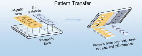
{"title":"范德华积分的模式转移","authors":"Zhen Hu, Ruo-Xuan Sun, Xu-Dong Chen, Jianguo Tian* and Zhibo Liu*, ","doi":"10.1021/acsaelm.4c0166410.1021/acsaelm.4c01664","DOIUrl":null,"url":null,"abstract":"<p >Atomically thin two-dimensional materials are promising candidates for designing functional electronic and optical devices through van der Waals integration. However, the route toward advanced devices typically involves transferring all prefabricated source materials onto target substrates, with significant reliance on post-transfer masking and etching operations to remove undesirable components. The existing transfer technologies are based on spin-coated polymeric carriers lacking controllable geometry, thereby limiting their ability to selectively transfer only the designated components of the source materials. Here, we introduce a pattern transfer technology for picking out the desired components from source materials on demand by rapidly patterning scalable polymeric transfer carriers into the required shapes and sizes. Patterned carriers provide the advantages of twist-angle controllability and one-step preparation of ready-to-transfer electrodes, enabling the formation of supermoiré homostructures and van der Waals electrical contacts. These capabilities of the pattern transfer technology offer great potential for the design and versatile integration of multifunctional van der Waals devices and drive forward the industrial application of two-dimensional materials.</p>","PeriodicalId":3,"journal":{"name":"ACS Applied Electronic Materials","volume":"6 11","pages":"8463–8473 8463–8473"},"PeriodicalIF":4.7000,"publicationDate":"2024-10-30","publicationTypes":"Journal Article","fieldsOfStudy":null,"isOpenAccess":false,"openAccessPdf":"","citationCount":"0","resultStr":"{\"title\":\"Pattern Transfer for van der Waals Integration\",\"authors\":\"Zhen Hu, Ruo-Xuan Sun, Xu-Dong Chen, Jianguo Tian* and Zhibo Liu*, \",\"doi\":\"10.1021/acsaelm.4c0166410.1021/acsaelm.4c01664\",\"DOIUrl\":null,\"url\":null,\"abstract\":\"<p >Atomically thin two-dimensional materials are promising candidates for designing functional electronic and optical devices through van der Waals integration. However, the route toward advanced devices typically involves transferring all prefabricated source materials onto target substrates, with significant reliance on post-transfer masking and etching operations to remove undesirable components. The existing transfer technologies are based on spin-coated polymeric carriers lacking controllable geometry, thereby limiting their ability to selectively transfer only the designated components of the source materials. Here, we introduce a pattern transfer technology for picking out the desired components from source materials on demand by rapidly patterning scalable polymeric transfer carriers into the required shapes and sizes. Patterned carriers provide the advantages of twist-angle controllability and one-step preparation of ready-to-transfer electrodes, enabling the formation of supermoiré homostructures and van der Waals electrical contacts. These capabilities of the pattern transfer technology offer great potential for the design and versatile integration of multifunctional van der Waals devices and drive forward the industrial application of two-dimensional materials.</p>\",\"PeriodicalId\":3,\"journal\":{\"name\":\"ACS Applied Electronic Materials\",\"volume\":\"6 11\",\"pages\":\"8463–8473 8463–8473\"},\"PeriodicalIF\":4.7000,\"publicationDate\":\"2024-10-30\",\"publicationTypes\":\"Journal Article\",\"fieldsOfStudy\":null,\"isOpenAccess\":false,\"openAccessPdf\":\"\",\"citationCount\":\"0\",\"resultStr\":null,\"platform\":\"Semanticscholar\",\"paperid\":null,\"PeriodicalName\":\"ACS Applied Electronic Materials\",\"FirstCategoryId\":\"88\",\"ListUrlMain\":\"https://pubs.acs.org/doi/10.1021/acsaelm.4c01664\",\"RegionNum\":3,\"RegionCategory\":\"材料科学\",\"ArticlePicture\":[],\"TitleCN\":null,\"AbstractTextCN\":null,\"PMCID\":null,\"EPubDate\":\"\",\"PubModel\":\"\",\"JCR\":\"Q1\",\"JCRName\":\"ENGINEERING, ELECTRICAL & ELECTRONIC\",\"Score\":null,\"Total\":0}","platform":"Semanticscholar","paperid":null,"PeriodicalName":"ACS Applied Electronic Materials","FirstCategoryId":"88","ListUrlMain":"https://pubs.acs.org/doi/10.1021/acsaelm.4c01664","RegionNum":3,"RegionCategory":"材料科学","ArticlePicture":[],"TitleCN":null,"AbstractTextCN":null,"PMCID":null,"EPubDate":"","PubModel":"","JCR":"Q1","JCRName":"ENGINEERING, ELECTRICAL & ELECTRONIC","Score":null,"Total":0}
Atomically thin two-dimensional materials are promising candidates for designing functional electronic and optical devices through van der Waals integration. However, the route toward advanced devices typically involves transferring all prefabricated source materials onto target substrates, with significant reliance on post-transfer masking and etching operations to remove undesirable components. The existing transfer technologies are based on spin-coated polymeric carriers lacking controllable geometry, thereby limiting their ability to selectively transfer only the designated components of the source materials. Here, we introduce a pattern transfer technology for picking out the desired components from source materials on demand by rapidly patterning scalable polymeric transfer carriers into the required shapes and sizes. Patterned carriers provide the advantages of twist-angle controllability and one-step preparation of ready-to-transfer electrodes, enabling the formation of supermoiré homostructures and van der Waals electrical contacts. These capabilities of the pattern transfer technology offer great potential for the design and versatile integration of multifunctional van der Waals devices and drive forward the industrial application of two-dimensional materials.
期刊介绍:
ACS Applied Electronic Materials is an interdisciplinary journal publishing original research covering all aspects of electronic materials. The journal is devoted to reports of new and original experimental and theoretical research of an applied nature that integrate knowledge in the areas of materials science, engineering, optics, physics, and chemistry into important applications of electronic materials. Sample research topics that span the journal's scope are inorganic, organic, ionic and polymeric materials with properties that include conducting, semiconducting, superconducting, insulating, dielectric, magnetic, optoelectronic, piezoelectric, ferroelectric and thermoelectric.
Indexed/Abstracted:
Web of Science SCIE
Scopus
CAS
INSPEC
Portico

 求助内容:
求助内容: 应助结果提醒方式:


