用飞秒激光制作的掺金黑硅光电探测器具有卓越的近红外响应能力

IF 8.3 2区 材料科学 Q1 MATERIALS SCIENCE, MULTIDISCIPLINARY
Wenpan Tao, Jingya Sun, Yifan Deng, Yiling Lian, Zhicheng Chen, Lan Jiang
{"title":"用飞秒激光制作的掺金黑硅光电探测器具有卓越的近红外响应能力","authors":"Wenpan Tao, Jingya Sun, Yifan Deng, Yiling Lian, Zhicheng Chen, Lan Jiang","doi":"10.1021/acsami.4c16830","DOIUrl":null,"url":null,"abstract":"Silicon photonic devices are key components in optical imaging and sensing for communication, and the development of silicon-based photodetectors with ideal performance in the visible and infrared spectral ranges can promote the application of silicon photonics in various photoelectronic systems. Here, a Au-doped black silicon photodetector was prepared by a femtosecond laser direct writing technique. The conical micro-/nanostructures with different sizes were produced by different laser fluence irradiation. Ultrafast pump–probe technology revealed that the strong spallation process and phase explosion between Au and silicon facilitate the interfusion of Au atoms into the silicon lattice. EDS analyses, Raman spectra, and XPS spectra show the uniform distribution of Au elements, multiconfiguration amorphous phase transition, and stable chemical valence states of Au elements in Au-doped black silicon layers, respectively. The excellent geometric light trapping performance of the surface conic structure-assisted photodetector achieved a high absorptance of 95% in the 200–1100 nm band. Simultaneously, the introduction of the intermediate band by Au hyperdoping also leads to a strong absorptance of 75% in the 1100–2500 nm band. The photoelectrical response rate of the Au-doped black silicon photodetectors increased by 10 times in the infrared wavelength band by means of the introduced intermediate energy levels through Au element doping. The switching photocurrent ratio is also found to be boosted 10 times, which comes from the reduction of the photon injection barrier. The excellent photoelectronic properties lead to the increased potential of femtosecond laser processing for integration with photonics and electronics, which shows great possibilities in the further progress of energy devices, information technology, and artificial intelligence.","PeriodicalId":5,"journal":{"name":"ACS Applied Materials & Interfaces","volume":null,"pages":null},"PeriodicalIF":8.3000,"publicationDate":"2024-11-13","publicationTypes":"Journal Article","fieldsOfStudy":null,"isOpenAccess":false,"openAccessPdf":"","citationCount":"0","resultStr":"{\"title\":\"Au-Doped Black Silicon Photodetector Fabricated by a Femtosecond Laser with Excellent Near-Infrared Response\",\"authors\":\"Wenpan Tao, Jingya Sun, Yifan Deng, Yiling Lian, Zhicheng Chen, Lan Jiang\",\"doi\":\"10.1021/acsami.4c16830\",\"DOIUrl\":null,\"url\":null,\"abstract\":\"Silicon photonic devices are key components in optical imaging and sensing for communication, and the development of silicon-based photodetectors with ideal performance in the visible and infrared spectral ranges can promote the application of silicon photonics in various photoelectronic systems. Here, a Au-doped black silicon photodetector was prepared by a femtosecond laser direct writing technique. The conical micro-/nanostructures with different sizes were produced by different laser fluence irradiation. Ultrafast pump–probe technology revealed that the strong spallation process and phase explosion between Au and silicon facilitate the interfusion of Au atoms into the silicon lattice. EDS analyses, Raman spectra, and XPS spectra show the uniform distribution of Au elements, multiconfiguration amorphous phase transition, and stable chemical valence states of Au elements in Au-doped black silicon layers, respectively. The excellent geometric light trapping performance of the surface conic structure-assisted photodetector achieved a high absorptance of 95% in the 200–1100 nm band. Simultaneously, the introduction of the intermediate band by Au hyperdoping also leads to a strong absorptance of 75% in the 1100–2500 nm band. The photoelectrical response rate of the Au-doped black silicon photodetectors increased by 10 times in the infrared wavelength band by means of the introduced intermediate energy levels through Au element doping. The switching photocurrent ratio is also found to be boosted 10 times, which comes from the reduction of the photon injection barrier. The excellent photoelectronic properties lead to the increased potential of femtosecond laser processing for integration with photonics and electronics, which shows great possibilities in the further progress of energy devices, information technology, and artificial intelligence.\",\"PeriodicalId\":5,\"journal\":{\"name\":\"ACS Applied Materials & Interfaces\",\"volume\":null,\"pages\":null},\"PeriodicalIF\":8.3000,\"publicationDate\":\"2024-11-13\",\"publicationTypes\":\"Journal Article\",\"fieldsOfStudy\":null,\"isOpenAccess\":false,\"openAccessPdf\":\"\",\"citationCount\":\"0\",\"resultStr\":null,\"platform\":\"Semanticscholar\",\"paperid\":null,\"PeriodicalName\":\"ACS Applied Materials & Interfaces\",\"FirstCategoryId\":\"88\",\"ListUrlMain\":\"https://doi.org/10.1021/acsami.4c16830\",\"RegionNum\":2,\"RegionCategory\":\"材料科学\",\"ArticlePicture\":[],\"TitleCN\":null,\"AbstractTextCN\":null,\"PMCID\":null,\"EPubDate\":\"\",\"PubModel\":\"\",\"JCR\":\"Q1\",\"JCRName\":\"MATERIALS SCIENCE, MULTIDISCIPLINARY\",\"Score\":null,\"Total\":0}","platform":"Semanticscholar","paperid":null,"PeriodicalName":"ACS Applied Materials & Interfaces","FirstCategoryId":"88","ListUrlMain":"https://doi.org/10.1021/acsami.4c16830","RegionNum":2,"RegionCategory":"材料科学","ArticlePicture":[],"TitleCN":null,"AbstractTextCN":null,"PMCID":null,"EPubDate":"","PubModel":"","JCR":"Q1","JCRName":"MATERIALS SCIENCE, MULTIDISCIPLINARY","Score":null,"Total":0}
引用次数: 0

摘要

硅光子器件是光学成像和通信传感中的关键元件,开发在可见光和红外光谱范围内性能理想的硅基光电探测器可以促进硅光子技术在各种光电子系统中的应用。本文采用飞秒激光直写技术制备了掺金黑硅光电探测器。在不同激光通量的照射下,制备出不同尺寸的锥形微/纳米结构。超快泵探技术表明,金与硅之间的强烈剥落过程和相爆促进了金原子与硅晶格的相互融合。EDS 分析、拉曼光谱和 XPS 光谱分别显示了掺金黑硅层中金元素的均匀分布、多构型非晶相变和稳定的金元素化合价态。表面圆锥结构辅助光电探测器具有优异的几何光捕获性能,在 200-1100 纳米波段的吸收率高达 95%。同时,通过金的超掺杂引入中间带,也在 1100-2500 纳米波段实现了 75% 的高吸收率。通过掺杂金元素引入中间能级,掺金黑硅光电探测器在红外波段的光电响应速度提高了 10 倍。开关光电流比也提高了 10 倍,这源于光子注入势垒的降低。优异的光电子特性提高了飞秒激光加工与光子学和电子学集成的潜力,为能源设备、信息技术和人工智能的进一步发展提供了巨大的可能性。
本文章由计算机程序翻译,如有差异,请以英文原文为准。

Au-Doped Black Silicon Photodetector Fabricated by a Femtosecond Laser with Excellent Near-Infrared Response

Au-Doped Black Silicon Photodetector Fabricated by a Femtosecond Laser with Excellent Near-Infrared Response
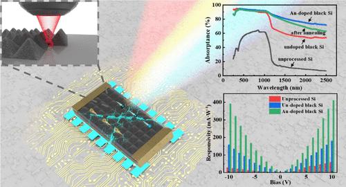
Silicon photonic devices are key components in optical imaging and sensing for communication, and the development of silicon-based photodetectors with ideal performance in the visible and infrared spectral ranges can promote the application of silicon photonics in various photoelectronic systems. Here, a Au-doped black silicon photodetector was prepared by a femtosecond laser direct writing technique. The conical micro-/nanostructures with different sizes were produced by different laser fluence irradiation. Ultrafast pump–probe technology revealed that the strong spallation process and phase explosion between Au and silicon facilitate the interfusion of Au atoms into the silicon lattice. EDS analyses, Raman spectra, and XPS spectra show the uniform distribution of Au elements, multiconfiguration amorphous phase transition, and stable chemical valence states of Au elements in Au-doped black silicon layers, respectively. The excellent geometric light trapping performance of the surface conic structure-assisted photodetector achieved a high absorptance of 95% in the 200–1100 nm band. Simultaneously, the introduction of the intermediate band by Au hyperdoping also leads to a strong absorptance of 75% in the 1100–2500 nm band. The photoelectrical response rate of the Au-doped black silicon photodetectors increased by 10 times in the infrared wavelength band by means of the introduced intermediate energy levels through Au element doping. The switching photocurrent ratio is also found to be boosted 10 times, which comes from the reduction of the photon injection barrier. The excellent photoelectronic properties lead to the increased potential of femtosecond laser processing for integration with photonics and electronics, which shows great possibilities in the further progress of energy devices, information technology, and artificial intelligence.
求助全文
通过发布文献求助,成功后即可免费获取论文全文。 去求助
来源期刊
ACS Applied Materials & Interfaces
ACS Applied Materials & Interfaces 工程技术-材料科学:综合
CiteScore
16.00
自引率
6.30%
发文量
4978
审稿时长
1.8 months
期刊介绍: ACS Applied Materials & Interfaces is a leading interdisciplinary journal that brings together chemists, engineers, physicists, and biologists to explore the development and utilization of newly-discovered materials and interfacial processes for specific applications. Our journal has experienced remarkable growth since its establishment in 2009, both in terms of the number of articles published and the impact of the research showcased. We are proud to foster a truly global community, with the majority of published articles originating from outside the United States, reflecting the rapid growth of applied research worldwide.
×
引用
GB/T 7714-2015
复制
MLA
复制
APA
复制
导出至
BibTeX EndNote RefMan NoteFirst NoteExpress
×
提示
您的信息不完整,为了账户安全,请先补充。
现在去补充
×
提示
您因"违规操作"
具体请查看互助需知
我知道了
×
提示
确定
请完成安全验证×
copy
已复制链接
快去分享给好友吧!
我知道了
右上角分享
点击右上角分享
0
联系我们:info@booksci.cn Book学术提供免费学术资源搜索服务,方便国内外学者检索中英文文献。致力于提供最便捷和优质的服务体验。 Copyright © 2023 布克学术 All rights reserved.
京ICP备2023020795号-1
ghs 京公网安备 11010802042870号
Book学术文献互助
Book学术文献互助群
群 号:481959085
Book学术官方微信