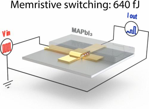
具有飞焦耳能耗的可扩展微尺度卤化铅包晶石人工突触

IF 19.3 1区 材料科学 Q1 CHEMISTRY, PHYSICAL
Jeroen J. de Boer, Bruno Ehrler
{"title":"具有飞焦耳能耗的可扩展微尺度卤化铅包晶石人工突触","authors":"Jeroen J. de Boer, Bruno Ehrler","doi":"10.1021/acsenergylett.4c02360","DOIUrl":null,"url":null,"abstract":"The efficient conduction of mobile ions in halide perovskites is highly promising for artificial synapses (or memristive devices), devices with a conductivity that can be varied by applying a bias voltage. Here we address the challenge of downscaling halide perovskite-based artificial synapses to achieve low energy consumption and allow high-density integration. We fabricate halide perovskite artificial synapses in a back-contacted architecture to achieve microscale devices despite the high solubility of halide perovskites in polar solvents that are commonly used in lithography. The energy consumption of a conductance change of the device is as low as 640 fJ, among the lowest reported for two-terminal halide perovskite artificial synapses so far. Moreover, the high resistance of the device up to hundreds of megaohms, low operating voltage of 100 mV and simple two-terminal architecture enable implementation in highly dense crossbar arrays. These arrays could potentially show orders of magnitude lower energy consumption for computation compared to conventional digital computers.","PeriodicalId":16,"journal":{"name":"ACS Energy Letters ","volume":"38 1","pages":""},"PeriodicalIF":19.3000,"publicationDate":"2024-11-08","publicationTypes":"Journal Article","fieldsOfStudy":null,"isOpenAccess":false,"openAccessPdf":"","citationCount":"0","resultStr":"{\"title\":\"Scalable Microscale Artificial Synapses of Lead Halide Perovskite with Femtojoule Energy Consumption\",\"authors\":\"Jeroen J. de Boer, Bruno Ehrler\",\"doi\":\"10.1021/acsenergylett.4c02360\",\"DOIUrl\":null,\"url\":null,\"abstract\":\"The efficient conduction of mobile ions in halide perovskites is highly promising for artificial synapses (or memristive devices), devices with a conductivity that can be varied by applying a bias voltage. Here we address the challenge of downscaling halide perovskite-based artificial synapses to achieve low energy consumption and allow high-density integration. We fabricate halide perovskite artificial synapses in a back-contacted architecture to achieve microscale devices despite the high solubility of halide perovskites in polar solvents that are commonly used in lithography. The energy consumption of a conductance change of the device is as low as 640 fJ, among the lowest reported for two-terminal halide perovskite artificial synapses so far. Moreover, the high resistance of the device up to hundreds of megaohms, low operating voltage of 100 mV and simple two-terminal architecture enable implementation in highly dense crossbar arrays. These arrays could potentially show orders of magnitude lower energy consumption for computation compared to conventional digital computers.\",\"PeriodicalId\":16,\"journal\":{\"name\":\"ACS Energy Letters \",\"volume\":\"38 1\",\"pages\":\"\"},\"PeriodicalIF\":19.3000,\"publicationDate\":\"2024-11-08\",\"publicationTypes\":\"Journal Article\",\"fieldsOfStudy\":null,\"isOpenAccess\":false,\"openAccessPdf\":\"\",\"citationCount\":\"0\",\"resultStr\":null,\"platform\":\"Semanticscholar\",\"paperid\":null,\"PeriodicalName\":\"ACS Energy Letters \",\"FirstCategoryId\":\"88\",\"ListUrlMain\":\"https://doi.org/10.1021/acsenergylett.4c02360\",\"RegionNum\":1,\"RegionCategory\":\"材料科学\",\"ArticlePicture\":[],\"TitleCN\":null,\"AbstractTextCN\":null,\"PMCID\":null,\"EPubDate\":\"\",\"PubModel\":\"\",\"JCR\":\"Q1\",\"JCRName\":\"CHEMISTRY, PHYSICAL\",\"Score\":null,\"Total\":0}","platform":"Semanticscholar","paperid":null,"PeriodicalName":"ACS Energy Letters ","FirstCategoryId":"88","ListUrlMain":"https://doi.org/10.1021/acsenergylett.4c02360","RegionNum":1,"RegionCategory":"材料科学","ArticlePicture":[],"TitleCN":null,"AbstractTextCN":null,"PMCID":null,"EPubDate":"","PubModel":"","JCR":"Q1","JCRName":"CHEMISTRY, PHYSICAL","Score":null,"Total":0}
引用次数: 0

摘要

卤化物过氧化物中移动离子的高效传导性对于人工突触(或忆阻器件)极具前景,这种器件的传导性可通过施加偏置电压而改变。在这里,我们要解决的难题是如何缩小基于卤化物透镜的人工突触的规模,以实现低能耗和高密度集成。尽管卤化物透镜在光刻技术中常用的极性溶剂中溶解度很高,但我们仍采用背接触结构制造出了卤化物透镜人工突触,从而实现了微尺度器件。该器件电导变化的能耗低至 640 fJ,是迄今为止报告的两端卤化物包晶石人工突触中能耗最低的器件之一。此外,该器件高达数百兆欧的高电阻、100 mV 的低工作电压以及简单的双端结构,都使其能够在高密度的交叉棒阵列中实现。与传统的数字计算机相比,这些阵列的计算能耗可能会低几个数量级。
本文章由计算机程序翻译,如有差异,请以英文原文为准。

Scalable Microscale Artificial Synapses of Lead Halide Perovskite with Femtojoule Energy Consumption

Scalable Microscale Artificial Synapses of Lead Halide Perovskite with Femtojoule Energy Consumption
The efficient conduction of mobile ions in halide perovskites is highly promising for artificial synapses (or memristive devices), devices with a conductivity that can be varied by applying a bias voltage. Here we address the challenge of downscaling halide perovskite-based artificial synapses to achieve low energy consumption and allow high-density integration. We fabricate halide perovskite artificial synapses in a back-contacted architecture to achieve microscale devices despite the high solubility of halide perovskites in polar solvents that are commonly used in lithography. The energy consumption of a conductance change of the device is as low as 640 fJ, among the lowest reported for two-terminal halide perovskite artificial synapses so far. Moreover, the high resistance of the device up to hundreds of megaohms, low operating voltage of 100 mV and simple two-terminal architecture enable implementation in highly dense crossbar arrays. These arrays could potentially show orders of magnitude lower energy consumption for computation compared to conventional digital computers.
求助全文
通过发布文献求助,成功后即可免费获取论文全文。 去求助
来源期刊
ACS Energy Letters
ACS Energy Letters Energy-Renewable Energy, Sustainability and the Environment
CiteScore
31.20
自引率
5.00%
发文量
469
审稿时长
1 months
期刊介绍: ACS Energy Letters is a monthly journal that publishes papers reporting new scientific advances in energy research. The journal focuses on topics that are of interest to scientists working in the fundamental and applied sciences. Rapid publication is a central criterion for acceptance, and the journal is known for its quick publication times, with an average of 4-6 weeks from submission to web publication in As Soon As Publishable format. ACS Energy Letters is ranked as the number one journal in the Web of Science Electrochemistry category. It also ranks within the top 10 journals for Physical Chemistry, Energy & Fuels, and Nanoscience & Nanotechnology. The journal offers several types of articles, including Letters, Energy Express, Perspectives, Reviews, Editorials, Viewpoints and Energy Focus. Additionally, authors have the option to submit videos that summarize or support the information presented in a Perspective or Review article, which can be highlighted on the journal's website. ACS Energy Letters is abstracted and indexed in Chemical Abstracts Service/SciFinder, EBSCO-summon, PubMed, Web of Science, Scopus and Portico.
×
引用
GB/T 7714-2015
复制
MLA
复制
APA
复制
导出至
BibTeX EndNote RefMan NoteFirst NoteExpress
×
提示
您的信息不完整,为了账户安全,请先补充。
现在去补充
×
提示
您因"违规操作"
具体请查看互助需知
我知道了
×
提示
确定
请完成安全验证×
copy
已复制链接
快去分享给好友吧!
我知道了
右上角分享
点击右上角分享
0
联系我们:info@booksci.cn Book学术提供免费学术资源搜索服务,方便国内外学者检索中英文文献。致力于提供最便捷和优质的服务体验。 Copyright © 2023 布克学术 All rights reserved.
京ICP备2023020795号-1
ghs 京公网安备 11010802042870号
Book学术文献互助
Book学术文献互助群
群 号:481959085
Book学术官方微信