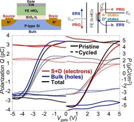
通过纳秒极化测量探究块状 Si:HfO2 FeFET 中电荷的来源

IF 2.6 4区 工程技术 Q2 ENGINEERING, ELECTRICAL & ELECTRONIC
Mor Mordechai Dahan , Halid Mulaosmanovic , Or Levit , Stefan Dünkel , Johannes Müller , Sven Beyer , Eilam Yalon
{"title":"通过纳秒极化测量探究块状 Si:HfO2 FeFET 中电荷的来源","authors":"Mor Mordechai Dahan ,&nbsp;Halid Mulaosmanovic ,&nbsp;Or Levit ,&nbsp;Stefan Dünkel ,&nbsp;Johannes Müller ,&nbsp;Sven Beyer ,&nbsp;Eilam Yalon","doi":"10.1016/j.mee.2024.112284","DOIUrl":null,"url":null,"abstract":"<div><div>FeFET technology offers the potential for fast, energy-efficient, low-cost, and high-capacity non-volatile memory and neuromorphic devices. However, charge trapping significantly affects device operation, leading to issues like read-after-write delay and limited endurance. Therefore, a detailed understanding of charge trapping, charge origin and its role in polarization switching is crucial. In this study, we uncover the spectral energy origin of polarization charges in Si:HfO<sub>2</sub> N-FeFET by probing electron (conduction band) and hole (valence band) currents separately during polarization-voltage (<em>P–V</em>) measurements. We utilize a fast (∼20 ns) and modified positive-up-negative-down (PUND) technique, where bulk, source, and drain currents of the FeFET are measured separately. The nanosecond timescale of the measurement results in measurable currents in FeFETs having dimensions of a few μm. This charge separation shows that program (PRG, <em>V</em><sub>GS</sub> &gt; 0) charge originates from the conduction band, whereas erase (ERS, <em>V</em><sub>GS</sub> &lt; 0) originates from the valence band of the Si. Moreover, the polarization curve (<em>P–V</em>) of a cycled device (following 5000 PRG/ERS pulses) shows measurable hysteresis even though the transfer curve of the same device shows that the memory window in the threshold voltage vanishes. Therefore, the FeFET polarization state can be read without delay after write operation by the fast PUND measurement, both for pristine and cycled FeFETs.</div></div>","PeriodicalId":18557,"journal":{"name":"Microelectronic Engineering","volume":null,"pages":null},"PeriodicalIF":2.6000,"publicationDate":"2024-11-06","publicationTypes":"Journal Article","fieldsOfStudy":null,"isOpenAccess":false,"openAccessPdf":"","citationCount":"0","resultStr":"{\"title\":\"Origin of charges in bulk Si:HfO2 FeFET probed by nanosecond polarization measurements\",\"authors\":\"Mor Mordechai Dahan ,&nbsp;Halid Mulaosmanovic ,&nbsp;Or Levit ,&nbsp;Stefan Dünkel ,&nbsp;Johannes Müller ,&nbsp;Sven Beyer ,&nbsp;Eilam Yalon\",\"doi\":\"10.1016/j.mee.2024.112284\",\"DOIUrl\":null,\"url\":null,\"abstract\":\"<div><div>FeFET technology offers the potential for fast, energy-efficient, low-cost, and high-capacity non-volatile memory and neuromorphic devices. However, charge trapping significantly affects device operation, leading to issues like read-after-write delay and limited endurance. Therefore, a detailed understanding of charge trapping, charge origin and its role in polarization switching is crucial. In this study, we uncover the spectral energy origin of polarization charges in Si:HfO<sub>2</sub> N-FeFET by probing electron (conduction band) and hole (valence band) currents separately during polarization-voltage (<em>P–V</em>) measurements. We utilize a fast (∼20 ns) and modified positive-up-negative-down (PUND) technique, where bulk, source, and drain currents of the FeFET are measured separately. The nanosecond timescale of the measurement results in measurable currents in FeFETs having dimensions of a few μm. This charge separation shows that program (PRG, <em>V</em><sub>GS</sub> &gt; 0) charge originates from the conduction band, whereas erase (ERS, <em>V</em><sub>GS</sub> &lt; 0) originates from the valence band of the Si. Moreover, the polarization curve (<em>P–V</em>) of a cycled device (following 5000 PRG/ERS pulses) shows measurable hysteresis even though the transfer curve of the same device shows that the memory window in the threshold voltage vanishes. Therefore, the FeFET polarization state can be read without delay after write operation by the fast PUND measurement, both for pristine and cycled FeFETs.</div></div>\",\"PeriodicalId\":18557,\"journal\":{\"name\":\"Microelectronic Engineering\",\"volume\":null,\"pages\":null},\"PeriodicalIF\":2.6000,\"publicationDate\":\"2024-11-06\",\"publicationTypes\":\"Journal Article\",\"fieldsOfStudy\":null,\"isOpenAccess\":false,\"openAccessPdf\":\"\",\"citationCount\":\"0\",\"resultStr\":null,\"platform\":\"Semanticscholar\",\"paperid\":null,\"PeriodicalName\":\"Microelectronic Engineering\",\"FirstCategoryId\":\"5\",\"ListUrlMain\":\"https://www.sciencedirect.com/science/article/pii/S0167931724001539\",\"RegionNum\":4,\"RegionCategory\":\"工程技术\",\"ArticlePicture\":[],\"TitleCN\":null,\"AbstractTextCN\":null,\"PMCID\":null,\"EPubDate\":\"\",\"PubModel\":\"\",\"JCR\":\"Q2\",\"JCRName\":\"ENGINEERING, ELECTRICAL & ELECTRONIC\",\"Score\":null,\"Total\":0}","platform":"Semanticscholar","paperid":null,"PeriodicalName":"Microelectronic Engineering","FirstCategoryId":"5","ListUrlMain":"https://www.sciencedirect.com/science/article/pii/S0167931724001539","RegionNum":4,"RegionCategory":"工程技术","ArticlePicture":[],"TitleCN":null,"AbstractTextCN":null,"PMCID":null,"EPubDate":"","PubModel":"","JCR":"Q2","JCRName":"ENGINEERING, ELECTRICAL & ELECTRONIC","Score":null,"Total":0}
引用次数: 0

摘要

FeFET 技术为快速、节能、低成本、高容量的非易失性存储器和神经形态器件提供了潜力。然而,电荷捕获会严重影响器件的运行,导致读写延迟和耐用性受限等问题。因此,详细了解电荷捕获、电荷起源及其在极化转换中的作用至关重要。在本研究中,我们通过在极化电压(P-V)测量过程中分别探测电子(导带)和空穴(价带)电流,揭示了 Si:HfO2 N-FeFET 中极化电荷的光谱能量来源。我们利用快速(∼20 ns)和改进的正上-负下(PUND)技术,分别测量 FeFET 的体电流、源电流和漏电流。测量的纳秒级时间尺度可测量出尺寸仅为几微米的 FeFET 中的电流。电荷分离表明,编程(PRG,VGS >0)电荷来自导带,而擦除(ERS,VGS <0)电荷来自硅的价带。此外,一个循环器件的极化曲线(P-V)(5000 PRG/ERS 脉冲之后)显示了可测量的滞后,尽管同一器件的转移曲线显示阈值电压的记忆窗口消失了。因此,通过快速 PUND 测量,可在写入操作后立即读取 FeFET 的极化状态,无论是原始 FeFET 还是循环 FeFET。
本文章由计算机程序翻译,如有差异,请以英文原文为准。

Origin of charges in bulk Si:HfO2 FeFET probed by nanosecond polarization measurements

Origin of charges in bulk Si:HfO2 FeFET probed by nanosecond polarization measurements
FeFET technology offers the potential for fast, energy-efficient, low-cost, and high-capacity non-volatile memory and neuromorphic devices. However, charge trapping significantly affects device operation, leading to issues like read-after-write delay and limited endurance. Therefore, a detailed understanding of charge trapping, charge origin and its role in polarization switching is crucial. In this study, we uncover the spectral energy origin of polarization charges in Si:HfO2 N-FeFET by probing electron (conduction band) and hole (valence band) currents separately during polarization-voltage (P–V) measurements. We utilize a fast (∼20 ns) and modified positive-up-negative-down (PUND) technique, where bulk, source, and drain currents of the FeFET are measured separately. The nanosecond timescale of the measurement results in measurable currents in FeFETs having dimensions of a few μm. This charge separation shows that program (PRG, VGS > 0) charge originates from the conduction band, whereas erase (ERS, VGS < 0) originates from the valence band of the Si. Moreover, the polarization curve (P–V) of a cycled device (following 5000 PRG/ERS pulses) shows measurable hysteresis even though the transfer curve of the same device shows that the memory window in the threshold voltage vanishes. Therefore, the FeFET polarization state can be read without delay after write operation by the fast PUND measurement, both for pristine and cycled FeFETs.
求助全文
通过发布文献求助,成功后即可免费获取论文全文。 去求助
来源期刊
Microelectronic Engineering
Microelectronic Engineering 工程技术-工程:电子与电气
CiteScore
5.30
自引率
4.30%
发文量
131
审稿时长
29 days
期刊介绍: Microelectronic Engineering is the premier nanoprocessing, and nanotechnology journal focusing on fabrication of electronic, photonic, bioelectronic, electromechanic and fluidic devices and systems, and their applications in the broad areas of electronics, photonics, energy, life sciences, and environment. It covers also the expanding interdisciplinary field of "more than Moore" and "beyond Moore" integrated nanoelectronics / photonics and micro-/nano-/bio-systems. Through its unique mixture of peer-reviewed articles, reviews, accelerated publications, short and Technical notes, and the latest research news on key developments, Microelectronic Engineering provides comprehensive coverage of this exciting, interdisciplinary and dynamic new field for researchers in academia and professionals in industry.
×
引用
GB/T 7714-2015
复制
MLA
复制
APA
复制
导出至
BibTeX EndNote RefMan NoteFirst NoteExpress
×
提示
您的信息不完整,为了账户安全,请先补充。
现在去补充
×
提示
您因"违规操作"
具体请查看互助需知
我知道了
×
提示
确定
请完成安全验证×
copy
已复制链接
快去分享给好友吧!
我知道了
右上角分享
点击右上角分享
0
联系我们:info@booksci.cn Book学术提供免费学术资源搜索服务,方便国内外学者检索中英文文献。致力于提供最便捷和优质的服务体验。 Copyright © 2023 布克学术 All rights reserved.
京ICP备2023020795号-1
ghs 京公网安备 11010802042870号
Book学术文献互助
Book学术文献互助群
群 号:481959085
Book学术官方微信