R. Corey White*, Morgan Bergthold, Aaron Muhowski, Leland Nordin, Iris Okoro, Hussein Hijazi, Leonard Feldman, Daniel Wasserman and Seth R. Bank,
{"title":"与 InSb 相匹配的 InAsSbBi 晶格的分子束外延,用于长波红外传感","authors":"R. Corey White*, Morgan Bergthold, Aaron Muhowski, Leland Nordin, Iris Okoro, Hussein Hijazi, Leonard Feldman, Daniel Wasserman and Seth R. Bank, ","doi":"10.1021/acs.cgd.4c0026410.1021/acs.cgd.4c00264","DOIUrl":null,"url":null,"abstract":"<p >InSb-based dilute-bismide alloys present a unique opportunity to span the entirety of the long-wave infrared with a bulk, lattice-matched III–V alloy that boasts greatly reduced toxicity compared to the current state-of-the-art, Hg<sub>1–<i>x</i></sub>Cd<sub><i>x</i></sub>Te. By incorporating both bismuth and arsenic in the appropriate proportions, we demonstrated InAs<sub>0.004</sub>Sb<sub>0.983</sub>Bi<sub>0.013</sub> lattice-matched to commercially available InSb substrates. A kinetically limited growth regime that combined low substrate temperatures, V/III flux ratios near unity, and a relatively fast growth rate, mitigated phase separation and resulted in films with excellent structural and optical quality. In particular, the bismuth incorporation was estimated to be approximately 95% substitutional and photoluminescence from the alloy was observed at elevated temperatures up to 400 K exhibiting significant wavelength extension beyond that of InSb, out to 7.6 μm at room temperature. Furthermore, the first antimony-rich InAs<sub><i>y</i></sub>Sb<sub>1–<i>x</i>–</sub><i><sub>y</sub></i>Bi<sub><i>x</i></sub> photodetector was fabricated and showed a longer cutoff wavelength than that of an InSb control detector due to the bandgap reduction caused by bismuth and arsenic incorporation. This highlights that emission and detection from InAs<sub>0.004</sub>Sb<sub>0.983</sub>Bi<sub>0.013</sub> have accessed the longest wavelengths of any lattice-matched, bulk III–V alloy to date. Altogether, these results demonstrate the strong potential of InAs<sub><i>y</i></sub>Sb<sub>1–<i>x</i>–</sub><i><sub>y</sub></i>Bi<sub><i>x</i></sub> for high-performance optoelectronic devices operating across the long-wave infrared.</p>","PeriodicalId":34,"journal":{"name":"Crystal Growth & Design","volume":"24 21","pages":"8727–8735 8727–8735"},"PeriodicalIF":3.4000,"publicationDate":"2024-10-23","publicationTypes":"Journal Article","fieldsOfStudy":null,"isOpenAccess":false,"openAccessPdf":"","citationCount":"0","resultStr":"{\"title\":\"Molecular Beam Epitaxy of InAsSbBi Lattice-Matched to InSb toward Long-Wave Infrared Sensing\",\"authors\":\"R. Corey White*, Morgan Bergthold, Aaron Muhowski, Leland Nordin, Iris Okoro, Hussein Hijazi, Leonard Feldman, Daniel Wasserman and Seth R. Bank, \",\"doi\":\"10.1021/acs.cgd.4c0026410.1021/acs.cgd.4c00264\",\"DOIUrl\":null,\"url\":null,\"abstract\":\"<p >InSb-based dilute-bismide alloys present a unique opportunity to span the entirety of the long-wave infrared with a bulk, lattice-matched III–V alloy that boasts greatly reduced toxicity compared to the current state-of-the-art, Hg<sub>1–<i>x</i></sub>Cd<sub><i>x</i></sub>Te. By incorporating both bismuth and arsenic in the appropriate proportions, we demonstrated InAs<sub>0.004</sub>Sb<sub>0.983</sub>Bi<sub>0.013</sub> lattice-matched to commercially available InSb substrates. A kinetically limited growth regime that combined low substrate temperatures, V/III flux ratios near unity, and a relatively fast growth rate, mitigated phase separation and resulted in films with excellent structural and optical quality. In particular, the bismuth incorporation was estimated to be approximately 95% substitutional and photoluminescence from the alloy was observed at elevated temperatures up to 400 K exhibiting significant wavelength extension beyond that of InSb, out to 7.6 μm at room temperature. Furthermore, the first antimony-rich InAs<sub><i>y</i></sub>Sb<sub>1–<i>x</i>–</sub><i><sub>y</sub></i>Bi<sub><i>x</i></sub> photodetector was fabricated and showed a longer cutoff wavelength than that of an InSb control detector due to the bandgap reduction caused by bismuth and arsenic incorporation. This highlights that emission and detection from InAs<sub>0.004</sub>Sb<sub>0.983</sub>Bi<sub>0.013</sub> have accessed the longest wavelengths of any lattice-matched, bulk III–V alloy to date. Altogether, these results demonstrate the strong potential of InAs<sub><i>y</i></sub>Sb<sub>1–<i>x</i>–</sub><i><sub>y</sub></i>Bi<sub><i>x</i></sub> for high-performance optoelectronic devices operating across the long-wave infrared.</p>\",\"PeriodicalId\":34,\"journal\":{\"name\":\"Crystal Growth & Design\",\"volume\":\"24 21\",\"pages\":\"8727–8735 8727–8735\"},\"PeriodicalIF\":3.4000,\"publicationDate\":\"2024-10-23\",\"publicationTypes\":\"Journal Article\",\"fieldsOfStudy\":null,\"isOpenAccess\":false,\"openAccessPdf\":\"\",\"citationCount\":\"0\",\"resultStr\":null,\"platform\":\"Semanticscholar\",\"paperid\":null,\"PeriodicalName\":\"Crystal Growth & Design\",\"FirstCategoryId\":\"92\",\"ListUrlMain\":\"https://pubs.acs.org/doi/10.1021/acs.cgd.4c00264\",\"RegionNum\":2,\"RegionCategory\":\"化学\",\"ArticlePicture\":[],\"TitleCN\":null,\"AbstractTextCN\":null,\"PMCID\":null,\"EPubDate\":\"\",\"PubModel\":\"\",\"JCR\":\"Q2\",\"JCRName\":\"CHEMISTRY, MULTIDISCIPLINARY\",\"Score\":null,\"Total\":0}","platform":"Semanticscholar","paperid":null,"PeriodicalName":"Crystal Growth & Design","FirstCategoryId":"92","ListUrlMain":"https://pubs.acs.org/doi/10.1021/acs.cgd.4c00264","RegionNum":2,"RegionCategory":"化学","ArticlePicture":[],"TitleCN":null,"AbstractTextCN":null,"PMCID":null,"EPubDate":"","PubModel":"","JCR":"Q2","JCRName":"CHEMISTRY, MULTIDISCIPLINARY","Score":null,"Total":0}
Molecular Beam Epitaxy of InAsSbBi Lattice-Matched to InSb toward Long-Wave Infrared Sensing
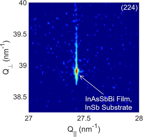
InSb-based dilute-bismide alloys present a unique opportunity to span the entirety of the long-wave infrared with a bulk, lattice-matched III–V alloy that boasts greatly reduced toxicity compared to the current state-of-the-art, Hg1–xCdxTe. By incorporating both bismuth and arsenic in the appropriate proportions, we demonstrated InAs0.004Sb0.983Bi0.013 lattice-matched to commercially available InSb substrates. A kinetically limited growth regime that combined low substrate temperatures, V/III flux ratios near unity, and a relatively fast growth rate, mitigated phase separation and resulted in films with excellent structural and optical quality. In particular, the bismuth incorporation was estimated to be approximately 95% substitutional and photoluminescence from the alloy was observed at elevated temperatures up to 400 K exhibiting significant wavelength extension beyond that of InSb, out to 7.6 μm at room temperature. Furthermore, the first antimony-rich InAsySb1–x–yBix photodetector was fabricated and showed a longer cutoff wavelength than that of an InSb control detector due to the bandgap reduction caused by bismuth and arsenic incorporation. This highlights that emission and detection from InAs0.004Sb0.983Bi0.013 have accessed the longest wavelengths of any lattice-matched, bulk III–V alloy to date. Altogether, these results demonstrate the strong potential of InAsySb1–x–yBix for high-performance optoelectronic devices operating across the long-wave infrared.
期刊介绍:
The aim of Crystal Growth & Design is to stimulate crossfertilization of knowledge among scientists and engineers working in the fields of crystal growth, crystal engineering, and the industrial application of crystalline materials.
Crystal Growth & Design publishes theoretical and experimental studies of the physical, chemical, and biological phenomena and processes related to the design, growth, and application of crystalline materials. Synergistic approaches originating from different disciplines and technologies and integrating the fields of crystal growth, crystal engineering, intermolecular interactions, and industrial application are encouraged.

 求助内容:
求助内容: 应助结果提醒方式:


