Elias Semlali*, Evelyne Gil, Geoffrey Avit, Yamina André, Arthur Sauvagnat, Jihen Jridi, Andriy V. Moskalenko, Philip A. Shields, Névine Rochat, Adeline Grenier and Agnès Trassoudaine*,
{"title":"在纳米尺度上控制 SAG-GaN","authors":"Elias Semlali*, Evelyne Gil, Geoffrey Avit, Yamina André, Arthur Sauvagnat, Jihen Jridi, Andriy V. Moskalenko, Philip A. Shields, Névine Rochat, Adeline Grenier and Agnès Trassoudaine*, ","doi":"10.1021/acs.cgd.4c0092510.1021/acs.cgd.4c00925","DOIUrl":null,"url":null,"abstract":"<p >Selective area growth (SAG) of GaN nanowires was performed on GaN on c-plane sapphire templates masked with SiN using hydride vapor phase epitaxy (HVPE). GaN nanowires exhibited various morphologies, discussed as a function of the pattern design, the partial pressure of the Ga gaseous precursor, the composition of the carrier gas, and the growth temperature. The morphologies are elucidated by involving a comparative study of growth rates of facets relative to each other. CL measurements showed high emission quality for GaN nanowires grown at 930 °C. This work places HVPE as an effective epitaxial technique for growing III–N nanostructure-based devices at a low cost.</p>","PeriodicalId":34,"journal":{"name":"Crystal Growth & Design","volume":"24 21","pages":"8907–8913 8907–8913"},"PeriodicalIF":3.2000,"publicationDate":"2024-10-09","publicationTypes":"Journal Article","fieldsOfStudy":null,"isOpenAccess":false,"openAccessPdf":"","citationCount":"0","resultStr":"{\"title\":\"Control of SAG-GaN at the Nanoscale\",\"authors\":\"Elias Semlali*, Evelyne Gil, Geoffrey Avit, Yamina André, Arthur Sauvagnat, Jihen Jridi, Andriy V. Moskalenko, Philip A. Shields, Névine Rochat, Adeline Grenier and Agnès Trassoudaine*, \",\"doi\":\"10.1021/acs.cgd.4c0092510.1021/acs.cgd.4c00925\",\"DOIUrl\":null,\"url\":null,\"abstract\":\"<p >Selective area growth (SAG) of GaN nanowires was performed on GaN on c-plane sapphire templates masked with SiN using hydride vapor phase epitaxy (HVPE). GaN nanowires exhibited various morphologies, discussed as a function of the pattern design, the partial pressure of the Ga gaseous precursor, the composition of the carrier gas, and the growth temperature. The morphologies are elucidated by involving a comparative study of growth rates of facets relative to each other. CL measurements showed high emission quality for GaN nanowires grown at 930 °C. This work places HVPE as an effective epitaxial technique for growing III–N nanostructure-based devices at a low cost.</p>\",\"PeriodicalId\":34,\"journal\":{\"name\":\"Crystal Growth & Design\",\"volume\":\"24 21\",\"pages\":\"8907–8913 8907–8913\"},\"PeriodicalIF\":3.2000,\"publicationDate\":\"2024-10-09\",\"publicationTypes\":\"Journal Article\",\"fieldsOfStudy\":null,\"isOpenAccess\":false,\"openAccessPdf\":\"\",\"citationCount\":\"0\",\"resultStr\":null,\"platform\":\"Semanticscholar\",\"paperid\":null,\"PeriodicalName\":\"Crystal Growth & Design\",\"FirstCategoryId\":\"92\",\"ListUrlMain\":\"https://pubs.acs.org/doi/10.1021/acs.cgd.4c00925\",\"RegionNum\":2,\"RegionCategory\":\"化学\",\"ArticlePicture\":[],\"TitleCN\":null,\"AbstractTextCN\":null,\"PMCID\":null,\"EPubDate\":\"\",\"PubModel\":\"\",\"JCR\":\"Q2\",\"JCRName\":\"CHEMISTRY, MULTIDISCIPLINARY\",\"Score\":null,\"Total\":0}","platform":"Semanticscholar","paperid":null,"PeriodicalName":"Crystal Growth & Design","FirstCategoryId":"92","ListUrlMain":"https://pubs.acs.org/doi/10.1021/acs.cgd.4c00925","RegionNum":2,"RegionCategory":"化学","ArticlePicture":[],"TitleCN":null,"AbstractTextCN":null,"PMCID":null,"EPubDate":"","PubModel":"","JCR":"Q2","JCRName":"CHEMISTRY, MULTIDISCIPLINARY","Score":null,"Total":0}
引用次数: 0
摘要
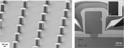
利用氢化物气相外延 (HVPE) 技术,在用氮化硅掩蔽的 c 平面蓝宝石模板上进行了氮化镓纳米线的选择性面积生长 (SAG)。GaN 纳米线呈现出各种形态,这些形态是图案设计、气态 Ga 前驱体的分压、载气成分和生长温度的函数。通过对各刻面相对生长速度的比较研究,阐明了这些形态。CL测量结果表明,在930 °C下生长的氮化镓纳米线具有较高的发射质量。这项研究将 HVPE 作为一种有效的外延技术,用于以低成本生长基于 III-N 纳米结构的器件。
Selective area growth (SAG) of GaN nanowires was performed on GaN on c-plane sapphire templates masked with SiN using hydride vapor phase epitaxy (HVPE). GaN nanowires exhibited various morphologies, discussed as a function of the pattern design, the partial pressure of the Ga gaseous precursor, the composition of the carrier gas, and the growth temperature. The morphologies are elucidated by involving a comparative study of growth rates of facets relative to each other. CL measurements showed high emission quality for GaN nanowires grown at 930 °C. This work places HVPE as an effective epitaxial technique for growing III–N nanostructure-based devices at a low cost.
期刊介绍:
The aim of Crystal Growth & Design is to stimulate crossfertilization of knowledge among scientists and engineers working in the fields of crystal growth, crystal engineering, and the industrial application of crystalline materials.
Crystal Growth & Design publishes theoretical and experimental studies of the physical, chemical, and biological phenomena and processes related to the design, growth, and application of crystalline materials. Synergistic approaches originating from different disciplines and technologies and integrating the fields of crystal growth, crystal engineering, intermolecular interactions, and industrial application are encouraged.