Muhammad Hussain, Sohail Abbas, Usama Waleed Qazi, Muhammad Riaz, Asif Ali, Fazal Wahab, Anis Fatima, Sajjad Hussain, Zdeněk Sofer and Jongwan Jung
{"title":"促进自偏压和高效近红外光电探测的 GeSe 嵌入金属氧化物双异质结。","authors":"Muhammad Hussain, Sohail Abbas, Usama Waleed Qazi, Muhammad Riaz, Asif Ali, Fazal Wahab, Anis Fatima, Sajjad Hussain, Zdeněk Sofer and Jongwan Jung","doi":"10.1039/D4NR03374D","DOIUrl":null,"url":null,"abstract":"<p >Infrared radiation detection is significantly important in communication, imaging, and sensing fields. Here, we present the integration of germanium selenide (GeSe) with a metal–oxide heterojunction to achieve efficient near-infrared (850 nm) photodetection under zero bias conditions. Nickel oxide (NiO) and silicon (Si) formed a favorable energy band alignment for the efficient separation of photogenerated charge carriers, resulting in a high figure of merits. The additional incorporation of a germanium selenide (GeSe) interlayer between the nickel oxide (NiO) and silicon (Si) heterojunction improved the external responsivity (from 0.22 to 3300 mA W<small><sup>−1</sup></small>), detectivity (from 1.24 × 10<small><sup>7</sup></small> to 20 × 10<small><sup>9</sup></small> Jones), normalized photocurrent to dark current ratio (from 4 × 10<small><sup>3</sup></small> to 3 × 10<small><sup>5</sup></small> W<small><sup>−1</sup></small>), noise equivalent power (from nW to pW), and rise/fall time (from 34/34.5 ms to 14/13 ms). The interlayer introduction of a semiconductor in various heterojunctions can facilitate self-biased and broadband photodetection for widely used optoelectronic applications.</p>","PeriodicalId":92,"journal":{"name":"Nanoscale","volume":" 48","pages":" 22267-22272"},"PeriodicalIF":5.1000,"publicationDate":"2024-11-05","publicationTypes":"Journal Article","fieldsOfStudy":null,"isOpenAccess":false,"openAccessPdf":"","citationCount":"0","resultStr":"{\"title\":\"GeSe-embedded metal–oxide double heterojunctions for facilitating self-biased and efficient NIR photodetection†\",\"authors\":\"Muhammad Hussain, Sohail Abbas, Usama Waleed Qazi, Muhammad Riaz, Asif Ali, Fazal Wahab, Anis Fatima, Sajjad Hussain, Zdeněk Sofer and Jongwan Jung\",\"doi\":\"10.1039/D4NR03374D\",\"DOIUrl\":null,\"url\":null,\"abstract\":\"<p >Infrared radiation detection is significantly important in communication, imaging, and sensing fields. Here, we present the integration of germanium selenide (GeSe) with a metal–oxide heterojunction to achieve efficient near-infrared (850 nm) photodetection under zero bias conditions. Nickel oxide (NiO) and silicon (Si) formed a favorable energy band alignment for the efficient separation of photogenerated charge carriers, resulting in a high figure of merits. The additional incorporation of a germanium selenide (GeSe) interlayer between the nickel oxide (NiO) and silicon (Si) heterojunction improved the external responsivity (from 0.22 to 3300 mA W<small><sup>−1</sup></small>), detectivity (from 1.24 × 10<small><sup>7</sup></small> to 20 × 10<small><sup>9</sup></small> Jones), normalized photocurrent to dark current ratio (from 4 × 10<small><sup>3</sup></small> to 3 × 10<small><sup>5</sup></small> W<small><sup>−1</sup></small>), noise equivalent power (from nW to pW), and rise/fall time (from 34/34.5 ms to 14/13 ms). The interlayer introduction of a semiconductor in various heterojunctions can facilitate self-biased and broadband photodetection for widely used optoelectronic applications.</p>\",\"PeriodicalId\":92,\"journal\":{\"name\":\"Nanoscale\",\"volume\":\" 48\",\"pages\":\" 22267-22272\"},\"PeriodicalIF\":5.1000,\"publicationDate\":\"2024-11-05\",\"publicationTypes\":\"Journal Article\",\"fieldsOfStudy\":null,\"isOpenAccess\":false,\"openAccessPdf\":\"\",\"citationCount\":\"0\",\"resultStr\":null,\"platform\":\"Semanticscholar\",\"paperid\":null,\"PeriodicalName\":\"Nanoscale\",\"FirstCategoryId\":\"88\",\"ListUrlMain\":\"https://pubs.rsc.org/en/content/articlelanding/2024/nr/d4nr03374d\",\"RegionNum\":3,\"RegionCategory\":\"材料科学\",\"ArticlePicture\":[],\"TitleCN\":null,\"AbstractTextCN\":null,\"PMCID\":null,\"EPubDate\":\"\",\"PubModel\":\"\",\"JCR\":\"Q1\",\"JCRName\":\"CHEMISTRY, MULTIDISCIPLINARY\",\"Score\":null,\"Total\":0}","platform":"Semanticscholar","paperid":null,"PeriodicalName":"Nanoscale","FirstCategoryId":"88","ListUrlMain":"https://pubs.rsc.org/en/content/articlelanding/2024/nr/d4nr03374d","RegionNum":3,"RegionCategory":"材料科学","ArticlePicture":[],"TitleCN":null,"AbstractTextCN":null,"PMCID":null,"EPubDate":"","PubModel":"","JCR":"Q1","JCRName":"CHEMISTRY, MULTIDISCIPLINARY","Score":null,"Total":0}
GeSe-embedded metal–oxide double heterojunctions for facilitating self-biased and efficient NIR photodetection†
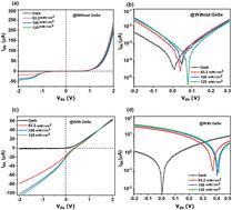
Infrared radiation detection is significantly important in communication, imaging, and sensing fields. Here, we present the integration of germanium selenide (GeSe) with a metal–oxide heterojunction to achieve efficient near-infrared (850 nm) photodetection under zero bias conditions. Nickel oxide (NiO) and silicon (Si) formed a favorable energy band alignment for the efficient separation of photogenerated charge carriers, resulting in a high figure of merits. The additional incorporation of a germanium selenide (GeSe) interlayer between the nickel oxide (NiO) and silicon (Si) heterojunction improved the external responsivity (from 0.22 to 3300 mA W−1), detectivity (from 1.24 × 10⁷ to 20 × 109 Jones), normalized photocurrent to dark current ratio (from 4 × 10³ to 3 × 10⁵ W−1), noise equivalent power (from nW to pW), and rise/fall time (from 34/34.5 ms to 14/13 ms). The interlayer introduction of a semiconductor in various heterojunctions can facilitate self-biased and broadband photodetection for widely used optoelectronic applications.
期刊介绍:
Nanoscale is a high-impact international journal, publishing high-quality research across nanoscience and nanotechnology. Nanoscale publishes a full mix of research articles on experimental and theoretical work, including reviews, communications, and full papers.Highly interdisciplinary, this journal appeals to scientists, researchers and professionals interested in nanoscience and nanotechnology, quantum materials and quantum technology, including the areas of physics, chemistry, biology, medicine, materials, energy/environment, information technology, detection science, healthcare and drug discovery, and electronics.

 求助内容:
求助内容: 应助结果提醒方式:


