Benjamin A. Chambers, Christopher T. Gibson and Gunther G. Andersson
{"title":"MoS2 薄膜的电子结构†","authors":"Benjamin A. Chambers, Christopher T. Gibson and Gunther G. Andersson","doi":"10.1039/D4LF00165F","DOIUrl":null,"url":null,"abstract":"<p >The valence electron structure of exfoliated monolayer MoS<small><sub>2</sub></small> deposited onto SiO<small><sub>2</sub></small> was determined by UV photoelectron spectroscopy through component analysis in combination with Auger electron microscopy. The valence electron cut-off for bulk MoS<small><sub>2</sub></small> was found at 0.64 eV binding energy whilst monolayer MoS<small><sub>2</sub></small> and few layer MoS<small><sub>2</sub></small> have higher binding energies of 0.89 eV and 1.26 eV respectively. SiO<small><sub>2</sub></small> is known to interact only weakly with MoS<small><sub>2</sub></small>. Thus, the valence electron structure of higher binding energy determined here is thus considered to represent that of a material not affected by strain. The implications of the change in the valence electron cut-off are discussed.</p>","PeriodicalId":101138,"journal":{"name":"RSC Applied Interfaces","volume":" 6","pages":" 1276-1284"},"PeriodicalIF":0.0000,"publicationDate":"2024-07-29","publicationTypes":"Journal Article","fieldsOfStudy":null,"isOpenAccess":false,"openAccessPdf":"https://pubs.rsc.org/en/content/articlepdf/2024/lf/d4lf00165f?page=search","citationCount":"0","resultStr":"{\"title\":\"Electronic structure of thin MoS2 films†\",\"authors\":\"Benjamin A. Chambers, Christopher T. Gibson and Gunther G. Andersson\",\"doi\":\"10.1039/D4LF00165F\",\"DOIUrl\":null,\"url\":null,\"abstract\":\"<p >The valence electron structure of exfoliated monolayer MoS<small><sub>2</sub></small> deposited onto SiO<small><sub>2</sub></small> was determined by UV photoelectron spectroscopy through component analysis in combination with Auger electron microscopy. The valence electron cut-off for bulk MoS<small><sub>2</sub></small> was found at 0.64 eV binding energy whilst monolayer MoS<small><sub>2</sub></small> and few layer MoS<small><sub>2</sub></small> have higher binding energies of 0.89 eV and 1.26 eV respectively. SiO<small><sub>2</sub></small> is known to interact only weakly with MoS<small><sub>2</sub></small>. Thus, the valence electron structure of higher binding energy determined here is thus considered to represent that of a material not affected by strain. The implications of the change in the valence electron cut-off are discussed.</p>\",\"PeriodicalId\":101138,\"journal\":{\"name\":\"RSC Applied Interfaces\",\"volume\":\" 6\",\"pages\":\" 1276-1284\"},\"PeriodicalIF\":0.0000,\"publicationDate\":\"2024-07-29\",\"publicationTypes\":\"Journal Article\",\"fieldsOfStudy\":null,\"isOpenAccess\":false,\"openAccessPdf\":\"https://pubs.rsc.org/en/content/articlepdf/2024/lf/d4lf00165f?page=search\",\"citationCount\":\"0\",\"resultStr\":null,\"platform\":\"Semanticscholar\",\"paperid\":null,\"PeriodicalName\":\"RSC Applied Interfaces\",\"FirstCategoryId\":\"1085\",\"ListUrlMain\":\"https://pubs.rsc.org/en/content/articlelanding/2024/lf/d4lf00165f\",\"RegionNum\":0,\"RegionCategory\":null,\"ArticlePicture\":[],\"TitleCN\":null,\"AbstractTextCN\":null,\"PMCID\":null,\"EPubDate\":\"\",\"PubModel\":\"\",\"JCR\":\"\",\"JCRName\":\"\",\"Score\":null,\"Total\":0}","platform":"Semanticscholar","paperid":null,"PeriodicalName":"RSC Applied Interfaces","FirstCategoryId":"1085","ListUrlMain":"https://pubs.rsc.org/en/content/articlelanding/2024/lf/d4lf00165f","RegionNum":0,"RegionCategory":null,"ArticlePicture":[],"TitleCN":null,"AbstractTextCN":null,"PMCID":null,"EPubDate":"","PubModel":"","JCR":"","JCRName":"","Score":null,"Total":0}
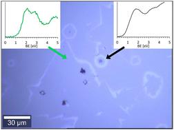
The valence electron structure of exfoliated monolayer MoS2 deposited onto SiO2 was determined by UV photoelectron spectroscopy through component analysis in combination with Auger electron microscopy. The valence electron cut-off for bulk MoS2 was found at 0.64 eV binding energy whilst monolayer MoS2 and few layer MoS2 have higher binding energies of 0.89 eV and 1.26 eV respectively. SiO2 is known to interact only weakly with MoS2. Thus, the valence electron structure of higher binding energy determined here is thus considered to represent that of a material not affected by strain. The implications of the change in the valence electron cut-off are discussed.

 求助内容:
求助内容: 应助结果提醒方式:


