Zhilong Wang, Sixian Liu, Kehao Tao, An Chen, Hongxiao Duan, Yanqiang Han, Fengqi You, Gang Liu, Jinjin Li
{"title":"电子材料生成的可解释替代学习。","authors":"Zhilong Wang, Sixian Liu, Kehao Tao, An Chen, Hongxiao Duan, Yanqiang Han, Fengqi You, Gang Liu, Jinjin Li","doi":"10.1021/acsnano.4c12166","DOIUrl":null,"url":null,"abstract":"<p><p>Despite many accessible AI models that have been developed, it is an open challenge to fully exploit interpretable insights to enable effective materials design and develop materials with desired properties for target applications. Here, we introduce an interpretable surrogate learning framework that can actively design and generate electronic materials (EMGen), akin to producing updated materials with requirements by screening all possible elements and fractions. Taking the materials system with required band gaps as a case study, EMGen exhibits a benchmarking predictive error and a running time of 1.7 min for designing and producing a structure with a desired band gap. Using EMGen, we establish a large hybrid functional band gap database, and more uplifting is that the proposed EMGen effectively designs Ga<sub><i>x</i></sub>O<sub><i>y</i></sub> with a wide band gap (>5.0 eV) for deep ultraviolet (DUV) optoelectronic devices, enabling a breakthrough extension of the applicability of Ga<sub><i>x</i></sub>O<sub><i>y</i></sub> films in photodetectors to DUV light below 240 nm. The augmented band gap also helps improve the breakdown voltage and the heat resilience performance of the amorphous Ga<sub><i>x</i></sub>O<sub><i>y</i></sub> film, thereby achieving considerable potential within the realm of power electronics applications. The proposed EMGen, as a specialized, interpretable AI model for the generation of electronic materials, is demonstrated to be an essential tool for on-demand semiconductor materials design.</p>","PeriodicalId":21,"journal":{"name":"ACS Nano","volume":" ","pages":"33587-33601"},"PeriodicalIF":16.0000,"publicationDate":"2024-12-10","publicationTypes":"Journal Article","fieldsOfStudy":null,"isOpenAccess":false,"openAccessPdf":"","citationCount":"0","resultStr":"{\"title\":\"Interpretable Surrogate Learning for Electronic Material Generation.\",\"authors\":\"Zhilong Wang, Sixian Liu, Kehao Tao, An Chen, Hongxiao Duan, Yanqiang Han, Fengqi You, Gang Liu, Jinjin Li\",\"doi\":\"10.1021/acsnano.4c12166\",\"DOIUrl\":null,\"url\":null,\"abstract\":\"<p><p>Despite many accessible AI models that have been developed, it is an open challenge to fully exploit interpretable insights to enable effective materials design and develop materials with desired properties for target applications. Here, we introduce an interpretable surrogate learning framework that can actively design and generate electronic materials (EMGen), akin to producing updated materials with requirements by screening all possible elements and fractions. Taking the materials system with required band gaps as a case study, EMGen exhibits a benchmarking predictive error and a running time of 1.7 min for designing and producing a structure with a desired band gap. Using EMGen, we establish a large hybrid functional band gap database, and more uplifting is that the proposed EMGen effectively designs Ga<sub><i>x</i></sub>O<sub><i>y</i></sub> with a wide band gap (>5.0 eV) for deep ultraviolet (DUV) optoelectronic devices, enabling a breakthrough extension of the applicability of Ga<sub><i>x</i></sub>O<sub><i>y</i></sub> films in photodetectors to DUV light below 240 nm. The augmented band gap also helps improve the breakdown voltage and the heat resilience performance of the amorphous Ga<sub><i>x</i></sub>O<sub><i>y</i></sub> film, thereby achieving considerable potential within the realm of power electronics applications. The proposed EMGen, as a specialized, interpretable AI model for the generation of electronic materials, is demonstrated to be an essential tool for on-demand semiconductor materials design.</p>\",\"PeriodicalId\":21,\"journal\":{\"name\":\"ACS Nano\",\"volume\":\" \",\"pages\":\"33587-33601\"},\"PeriodicalIF\":16.0000,\"publicationDate\":\"2024-12-10\",\"publicationTypes\":\"Journal Article\",\"fieldsOfStudy\":null,\"isOpenAccess\":false,\"openAccessPdf\":\"\",\"citationCount\":\"0\",\"resultStr\":null,\"platform\":\"Semanticscholar\",\"paperid\":null,\"PeriodicalName\":\"ACS Nano\",\"FirstCategoryId\":\"88\",\"ListUrlMain\":\"https://doi.org/10.1021/acsnano.4c12166\",\"RegionNum\":1,\"RegionCategory\":\"材料科学\",\"ArticlePicture\":[],\"TitleCN\":null,\"AbstractTextCN\":null,\"PMCID\":null,\"EPubDate\":\"2024/11/1 0:00:00\",\"PubModel\":\"Epub\",\"JCR\":\"Q1\",\"JCRName\":\"CHEMISTRY, MULTIDISCIPLINARY\",\"Score\":null,\"Total\":0}","platform":"Semanticscholar","paperid":null,"PeriodicalName":"ACS Nano","FirstCategoryId":"88","ListUrlMain":"https://doi.org/10.1021/acsnano.4c12166","RegionNum":1,"RegionCategory":"材料科学","ArticlePicture":[],"TitleCN":null,"AbstractTextCN":null,"PMCID":null,"EPubDate":"2024/11/1 0:00:00","PubModel":"Epub","JCR":"Q1","JCRName":"CHEMISTRY, MULTIDISCIPLINARY","Score":null,"Total":0}
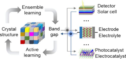
Interpretable Surrogate Learning for Electronic Material Generation.
Despite many accessible AI models that have been developed, it is an open challenge to fully exploit interpretable insights to enable effective materials design and develop materials with desired properties for target applications. Here, we introduce an interpretable surrogate learning framework that can actively design and generate electronic materials (EMGen), akin to producing updated materials with requirements by screening all possible elements and fractions. Taking the materials system with required band gaps as a case study, EMGen exhibits a benchmarking predictive error and a running time of 1.7 min for designing and producing a structure with a desired band gap. Using EMGen, we establish a large hybrid functional band gap database, and more uplifting is that the proposed EMGen effectively designs GaxOy with a wide band gap (>5.0 eV) for deep ultraviolet (DUV) optoelectronic devices, enabling a breakthrough extension of the applicability of GaxOy films in photodetectors to DUV light below 240 nm. The augmented band gap also helps improve the breakdown voltage and the heat resilience performance of the amorphous GaxOy film, thereby achieving considerable potential within the realm of power electronics applications. The proposed EMGen, as a specialized, interpretable AI model for the generation of electronic materials, is demonstrated to be an essential tool for on-demand semiconductor materials design.
期刊介绍:
ACS Nano, published monthly, serves as an international forum for comprehensive articles on nanoscience and nanotechnology research at the intersections of chemistry, biology, materials science, physics, and engineering. The journal fosters communication among scientists in these communities, facilitating collaboration, new research opportunities, and advancements through discoveries. ACS Nano covers synthesis, assembly, characterization, theory, and simulation of nanostructures, nanobiotechnology, nanofabrication, methods and tools for nanoscience and nanotechnology, and self- and directed-assembly. Alongside original research articles, it offers thorough reviews, perspectives on cutting-edge research, and discussions envisioning the future of nanoscience and nanotechnology.

 求助内容:
求助内容: 应助结果提醒方式:


