探测电荷阱存储器应用中非晶氮化硅隙内缺陷态的先进光谱方法

IF 2.4 4区 物理与天体物理 Q3 MATERIALS SCIENCE, MULTIDISCIPLINARY
{"title":"探测电荷阱存储器应用中非晶氮化硅隙内缺陷态的先进光谱方法","authors":"","doi":"10.1016/j.cap.2024.10.007","DOIUrl":null,"url":null,"abstract":"<div><div>Silicon nitride (SiN<sub>x</sub>) serves as the charge trap layer in current 3D NAND flash memory devices. The precise formation mechanism and electronic structure of localized defect trap states in SiN<sub>x</sub> remain elusive. Here, we present a refined experimental methodology to elucidate the in-gap defect states and the band gaps in amorphous SiN<sub>x</sub> thin films. Our approach integrates high-resolution reflection electron energy loss spectroscopy (REELS) and spectroscopic ellipsometry (SE) for comprehensive analysis. By systematical analysis, we aim to provide a robust method for determining in-gap electronic states in SiN<sub>x</sub>. We investigated two different SiN<sub>x</sub> films prepared by plasma-enhanced chemical vapor deposition and sputtering. Our analysis revealed several distinct in-gap states and determined band gap energies. This approach not only provide advanced spectroscopic methods to characterize the defect electronic states in SiN<sub>x</sub>, but also applicable to other large band gap semiconductors or dielectrics to predict device-level characteristics for future devices.</div></div>","PeriodicalId":11037,"journal":{"name":"Current Applied Physics","volume":null,"pages":null},"PeriodicalIF":2.4000,"publicationDate":"2024-10-24","publicationTypes":"Journal Article","fieldsOfStudy":null,"isOpenAccess":false,"openAccessPdf":"","citationCount":"0","resultStr":"{\"title\":\"Advanced spectroscopic methods for probing in-gap defect states in amorphous SiNx for charge trap memory applications\",\"authors\":\"\",\"doi\":\"10.1016/j.cap.2024.10.007\",\"DOIUrl\":null,\"url\":null,\"abstract\":\"<div><div>Silicon nitride (SiN<sub>x</sub>) serves as the charge trap layer in current 3D NAND flash memory devices. The precise formation mechanism and electronic structure of localized defect trap states in SiN<sub>x</sub> remain elusive. Here, we present a refined experimental methodology to elucidate the in-gap defect states and the band gaps in amorphous SiN<sub>x</sub> thin films. Our approach integrates high-resolution reflection electron energy loss spectroscopy (REELS) and spectroscopic ellipsometry (SE) for comprehensive analysis. By systematical analysis, we aim to provide a robust method for determining in-gap electronic states in SiN<sub>x</sub>. We investigated two different SiN<sub>x</sub> films prepared by plasma-enhanced chemical vapor deposition and sputtering. Our analysis revealed several distinct in-gap states and determined band gap energies. This approach not only provide advanced spectroscopic methods to characterize the defect electronic states in SiN<sub>x</sub>, but also applicable to other large band gap semiconductors or dielectrics to predict device-level characteristics for future devices.</div></div>\",\"PeriodicalId\":11037,\"journal\":{\"name\":\"Current Applied Physics\",\"volume\":null,\"pages\":null},\"PeriodicalIF\":2.4000,\"publicationDate\":\"2024-10-24\",\"publicationTypes\":\"Journal Article\",\"fieldsOfStudy\":null,\"isOpenAccess\":false,\"openAccessPdf\":\"\",\"citationCount\":\"0\",\"resultStr\":null,\"platform\":\"Semanticscholar\",\"paperid\":null,\"PeriodicalName\":\"Current Applied Physics\",\"FirstCategoryId\":\"101\",\"ListUrlMain\":\"https://www.sciencedirect.com/science/article/pii/S1567173924002219\",\"RegionNum\":4,\"RegionCategory\":\"物理与天体物理\",\"ArticlePicture\":[],\"TitleCN\":null,\"AbstractTextCN\":null,\"PMCID\":null,\"EPubDate\":\"\",\"PubModel\":\"\",\"JCR\":\"Q3\",\"JCRName\":\"MATERIALS SCIENCE, MULTIDISCIPLINARY\",\"Score\":null,\"Total\":0}","platform":"Semanticscholar","paperid":null,"PeriodicalName":"Current Applied Physics","FirstCategoryId":"101","ListUrlMain":"https://www.sciencedirect.com/science/article/pii/S1567173924002219","RegionNum":4,"RegionCategory":"物理与天体物理","ArticlePicture":[],"TitleCN":null,"AbstractTextCN":null,"PMCID":null,"EPubDate":"","PubModel":"","JCR":"Q3","JCRName":"MATERIALS SCIENCE, MULTIDISCIPLINARY","Score":null,"Total":0}
引用次数: 0

摘要

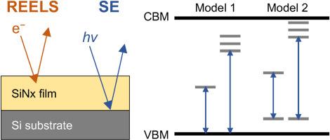
氮化硅(SiNx)是当前三维 NAND 闪存设备中的电荷陷阱层。氮化硅中局部缺陷陷阱态的精确形成机制和电子结构仍然难以捉摸。在此,我们提出了一种精炼的实验方法来阐明非晶 SiNx 薄膜中的隙内缺陷态和带隙。我们的方法整合了高分辨率反射电子能量损失光谱(REELS)和光谱椭偏仪(SE)进行综合分析。通过系统分析,我们旨在为确定 SiNx 的隙内电子状态提供一种可靠的方法。我们研究了通过等离子体增强化学气相沉积和溅射法制备的两种不同的 SiNx 薄膜。我们的分析揭示了几种不同的隙内态,并确定了带隙能量。这种方法不仅提供了表征 SiNx 中缺陷电子态的先进光谱方法,而且适用于其他大带隙半导体或电介质,以预测未来设备的器件级特性。
本文章由计算机程序翻译,如有差异,请以英文原文为准。

Advanced spectroscopic methods for probing in-gap defect states in amorphous SiNx for charge trap memory applications

Advanced spectroscopic methods for probing in-gap defect states in amorphous SiNx for charge trap memory applications
Silicon nitride (SiNx) serves as the charge trap layer in current 3D NAND flash memory devices. The precise formation mechanism and electronic structure of localized defect trap states in SiNx remain elusive. Here, we present a refined experimental methodology to elucidate the in-gap defect states and the band gaps in amorphous SiNx thin films. Our approach integrates high-resolution reflection electron energy loss spectroscopy (REELS) and spectroscopic ellipsometry (SE) for comprehensive analysis. By systematical analysis, we aim to provide a robust method for determining in-gap electronic states in SiNx. We investigated two different SiNx films prepared by plasma-enhanced chemical vapor deposition and sputtering. Our analysis revealed several distinct in-gap states and determined band gap energies. This approach not only provide advanced spectroscopic methods to characterize the defect electronic states in SiNx, but also applicable to other large band gap semiconductors or dielectrics to predict device-level characteristics for future devices.
求助全文
通过发布文献求助,成功后即可免费获取论文全文。 去求助
来源期刊
Current Applied Physics
Current Applied Physics 物理-材料科学:综合
CiteScore
4.80
自引率
0.00%
发文量
213
审稿时长
33 days
期刊介绍: Current Applied Physics (Curr. Appl. Phys.) is a monthly published international journal covering all the fields of applied science investigating the physics of the advanced materials for future applications. Other areas covered: Experimental and theoretical aspects of advanced materials and devices dealing with synthesis or structural chemistry, physical and electronic properties, photonics, engineering applications, and uniquely pertinent measurement or analytical techniques. Current Applied Physics, published since 2001, covers physics, chemistry and materials science, including bio-materials, with their engineering aspects. It is a truly interdisciplinary journal opening a forum for scientists of all related fields, a unique point of the journal discriminating it from other worldwide and/or Pacific Rim applied physics journals. Regular research papers, letters and review articles with contents meeting the scope of the journal will be considered for publication after peer review. The Journal is owned by the Korean Physical Society.
×
引用
GB/T 7714-2015
复制
MLA
复制
APA
复制
导出至
BibTeX EndNote RefMan NoteFirst NoteExpress
×
提示
您的信息不完整,为了账户安全,请先补充。
现在去补充
×
提示
您因"违规操作"
具体请查看互助需知
我知道了
×
提示
确定
请完成安全验证×
copy
已复制链接
快去分享给好友吧!
我知道了
右上角分享
点击右上角分享
0
联系我们:info@booksci.cn Book学术提供免费学术资源搜索服务,方便国内外学者检索中英文文献。致力于提供最便捷和优质的服务体验。 Copyright © 2023 布克学术 All rights reserved.
京ICP备2023020795号-1
ghs 京公网安备 11010802042870号
Book学术文献互助
Book学术文献互助群
群 号:481959085
Book学术官方微信