{"title":"增强喷雾沉积掺锑氧化锡薄膜的光电特性","authors":"B. Salameh , A.M. Alsmadi","doi":"10.1016/j.surfin.2024.105327","DOIUrl":null,"url":null,"abstract":"<div><div>Antimony-doped tin oxide (Sb:SnO<sub>2</sub>) thin films with varying Sb concentrations were deposited using the spray pyrolysis technique. A comprehensive analysis of the films' elemental, structural, and optoelectronic properties is presented. All films possess a polycrystalline single-phase nature and have a tetragonal rutile structure. As Sb concentration increases, the unit cell shrinks continuously, suggesting proper substitution of Sn<sup>4+</sup> by Sb<sup>5+</sup>. This substitution causes a continuous increase in the concentration of charge carriers and a reduction in electron mobility. X-ray photoelectron spectroscopy investigations revealed the presence of asymmetric Sn 3d core-level peaks distinguished by peak splitting, which increases with increasing carrier concentration. Utilizing the plasmon absorption model, an effective mass value of (0.51 ± 0.07)<em>m<sub>e</sub></em> for the conduction electron at the fermi level is obtained. With increasing Sb concentration, the optical energy gap increases gradually from 3.84 eV for undoped SnO<sub>2</sub> to 4.35 eV for 5.0 at. % Sb. After considering the Urbach tailing phenomenon as well as the Moss–Burstein effect, this increase was attributed to the increase in Moss–Burstein energy due to increased charge carrier concentration. Our study revealed that the film doped with 2.0 at. % Sb has the best optoelectronic properties, with a figure of merit of 4.18 (Ω/<em>cm</em><sup>2</sup>)<sup>−1</sup>.</div></div>","PeriodicalId":22081,"journal":{"name":"Surfaces and Interfaces","volume":"55 ","pages":"Article 105327"},"PeriodicalIF":5.7000,"publicationDate":"2024-10-28","publicationTypes":"Journal Article","fieldsOfStudy":null,"isOpenAccess":false,"openAccessPdf":"","citationCount":"0","resultStr":"{\"title\":\"Enhanced optoelectronic properties of spray deposited antimony-doped tin oxide thin films\",\"authors\":\"B. Salameh , A.M. Alsmadi\",\"doi\":\"10.1016/j.surfin.2024.105327\",\"DOIUrl\":null,\"url\":null,\"abstract\":\"<div><div>Antimony-doped tin oxide (Sb:SnO<sub>2</sub>) thin films with varying Sb concentrations were deposited using the spray pyrolysis technique. A comprehensive analysis of the films' elemental, structural, and optoelectronic properties is presented. All films possess a polycrystalline single-phase nature and have a tetragonal rutile structure. As Sb concentration increases, the unit cell shrinks continuously, suggesting proper substitution of Sn<sup>4+</sup> by Sb<sup>5+</sup>. This substitution causes a continuous increase in the concentration of charge carriers and a reduction in electron mobility. X-ray photoelectron spectroscopy investigations revealed the presence of asymmetric Sn 3d core-level peaks distinguished by peak splitting, which increases with increasing carrier concentration. Utilizing the plasmon absorption model, an effective mass value of (0.51 ± 0.07)<em>m<sub>e</sub></em> for the conduction electron at the fermi level is obtained. With increasing Sb concentration, the optical energy gap increases gradually from 3.84 eV for undoped SnO<sub>2</sub> to 4.35 eV for 5.0 at. % Sb. After considering the Urbach tailing phenomenon as well as the Moss–Burstein effect, this increase was attributed to the increase in Moss–Burstein energy due to increased charge carrier concentration. Our study revealed that the film doped with 2.0 at. % Sb has the best optoelectronic properties, with a figure of merit of 4.18 (Ω/<em>cm</em><sup>2</sup>)<sup>−1</sup>.</div></div>\",\"PeriodicalId\":22081,\"journal\":{\"name\":\"Surfaces and Interfaces\",\"volume\":\"55 \",\"pages\":\"Article 105327\"},\"PeriodicalIF\":5.7000,\"publicationDate\":\"2024-10-28\",\"publicationTypes\":\"Journal Article\",\"fieldsOfStudy\":null,\"isOpenAccess\":false,\"openAccessPdf\":\"\",\"citationCount\":\"0\",\"resultStr\":null,\"platform\":\"Semanticscholar\",\"paperid\":null,\"PeriodicalName\":\"Surfaces and Interfaces\",\"FirstCategoryId\":\"88\",\"ListUrlMain\":\"https://www.sciencedirect.com/science/article/pii/S2468023024014834\",\"RegionNum\":2,\"RegionCategory\":\"材料科学\",\"ArticlePicture\":[],\"TitleCN\":null,\"AbstractTextCN\":null,\"PMCID\":null,\"EPubDate\":\"\",\"PubModel\":\"\",\"JCR\":\"Q2\",\"JCRName\":\"CHEMISTRY, PHYSICAL\",\"Score\":null,\"Total\":0}","platform":"Semanticscholar","paperid":null,"PeriodicalName":"Surfaces and Interfaces","FirstCategoryId":"88","ListUrlMain":"https://www.sciencedirect.com/science/article/pii/S2468023024014834","RegionNum":2,"RegionCategory":"材料科学","ArticlePicture":[],"TitleCN":null,"AbstractTextCN":null,"PMCID":null,"EPubDate":"","PubModel":"","JCR":"Q2","JCRName":"CHEMISTRY, PHYSICAL","Score":null,"Total":0}
引用次数: 0
摘要
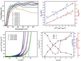
利用喷雾热解技术沉积了不同锑浓度的掺锑氧化锡(Sb:SnO2)薄膜。本文对薄膜的元素、结构和光电特性进行了全面分析。所有薄膜都具有多晶单相性质,并具有四方金红石结构。随着锑浓度的增加,单位晶胞不断缩小,这表明 Sb5+ 适当地取代了 Sn4+。这种置换导致电荷载流子浓度持续上升,电子迁移率降低。X 射线光电子能谱研究表明,存在非对称的 Sn 3d 核心级峰,其区别在于峰分裂,且随着载流子浓度的增加而增加。利用等离子体吸收模型,得到费米级传导电子的有效质量值为 (0.51 ± 0.07)me。随着掺锑浓度的增加,光学能隙从未掺锑二氧化锡的 3.84 eV 逐渐增加到掺锑 5.0 at.在考虑了乌尔巴赫拖尾现象和莫斯-伯斯坦效应后,这一增加归因于电荷载流子浓度增加导致的莫斯-伯斯坦能的增加。我们的研究表明,掺杂 2.0%锑的薄膜具有最佳的光电特性,其优越性为 4.18 (Ω/cm2)-1。
Enhanced optoelectronic properties of spray deposited antimony-doped tin oxide thin films
Antimony-doped tin oxide (Sb:SnO2) thin films with varying Sb concentrations were deposited using the spray pyrolysis technique. A comprehensive analysis of the films' elemental, structural, and optoelectronic properties is presented. All films possess a polycrystalline single-phase nature and have a tetragonal rutile structure. As Sb concentration increases, the unit cell shrinks continuously, suggesting proper substitution of Sn4+ by Sb5+. This substitution causes a continuous increase in the concentration of charge carriers and a reduction in electron mobility. X-ray photoelectron spectroscopy investigations revealed the presence of asymmetric Sn 3d core-level peaks distinguished by peak splitting, which increases with increasing carrier concentration. Utilizing the plasmon absorption model, an effective mass value of (0.51 ± 0.07)me for the conduction electron at the fermi level is obtained. With increasing Sb concentration, the optical energy gap increases gradually from 3.84 eV for undoped SnO2 to 4.35 eV for 5.0 at. % Sb. After considering the Urbach tailing phenomenon as well as the Moss–Burstein effect, this increase was attributed to the increase in Moss–Burstein energy due to increased charge carrier concentration. Our study revealed that the film doped with 2.0 at. % Sb has the best optoelectronic properties, with a figure of merit of 4.18 (Ω/cm2)−1.
期刊介绍:
The aim of the journal is to provide a respectful outlet for ''sound science'' papers in all research areas on surfaces and interfaces. We define sound science papers as papers that describe new and well-executed research, but that do not necessarily provide brand new insights or are merely a description of research results.
Surfaces and Interfaces publishes research papers in all fields of surface science which may not always find the right home on first submission to our Elsevier sister journals (Applied Surface, Surface and Coatings Technology, Thin Solid Films)