在多晶 Si3N4 衬底上溅射 (111) 高取向纳米细化银,用于大功率电子封装
IF 5.7
2区 材料科学
Q2 CHEMISTRY, PHYSICAL
引用次数: 0
摘要
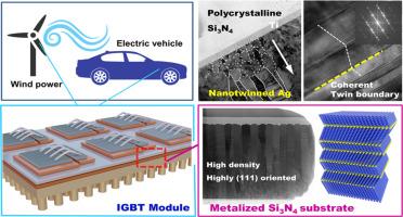
纳米银(NT-Ag)具有优异的机械和电气性能,这要归功于它在纳米尺度上的高密度和(111)高取向孪晶结构。因此,它最近在电子封装领域备受关注,可用作互连或金属化材料。然而,如何在多晶陶瓷基底上制备高密度、高取向的 NT-Ag 却一直是一个严峻的挑战,因为陶瓷基底的晶体结构并不支持 NT-Ag 薄膜的外延生长。本研究采用磁控溅射法在多晶陶瓷基底上制备了高密度、高取向性的 NT-Ag 薄膜,即氮化硅上的 NT-Ag(NT-Ag@Si3N4)。研究结果表明,在沿生长方向排列的柱状晶粒中,出现了紧密堆积的高密度 NT-Ag,NT-Ag 薄膜的纳米压痕硬度达到 1.82 GPa,电阻率为 2.06 μ‧Ωcm。此外,本研究还讨论并解释了通过控制磁控溅射工艺参数(如溅射功率和氩气流速)来实现 NT-Ag 薄膜生长的动力学和机制。此外,还研究了 NT-Ag 在 (100) Si 和多晶 Si3N4 上生长机制的差异。凭借其优异的材料特性,NT-Ag@Si3N4 在大功率电子产品的先进封装技术应用中大有可为。本文章由计算机程序翻译,如有差异,请以英文原文为准。
Sputtering of (111) highly-oriented nanotwinned Ag on polycrystalline Si3N4 substrates for high-power electronic packaging
Nanotwinned silver (NT-Ag) exhibits excellent mechanical and electrical properties, attributed to its high-density and (111) highly-oriented twinning structure in nanoscale. Therefore, it has recently drawn much attention in the field of electronic packaging, where it can be utilized as interconnection or metallization materials. However, it has been a critical challenge to fabricate the high-density and highly-oriented NT-Ag onto polycrystalline ceramic substrates, whose crystal structure does not support the epitaxial growth of NT-Ag films. In the current work, a high-density and highly-oriented NT-Ag film has been fabricated onto a polycrystalline ceramic substrate, i.e., NT-Ag on silicon nitride (NT-Ag@Si3N4), using the magnetron sputtering method. As results, a close-packed arrangement of high-density NT-Ag has been observed within columnar grains aligned along its growth direction, whereas the nanoindentation hardness of the NT-Ag film reached 1.82 GPa, with an electrical resistivity of 2.06 μΩ‧cm. Moreover, this study has discussed and explained the growth kinetics and mechanism of NT-Ag films, by controlling magnetron sputtering process parameters, such as sputtering power and argon flow rate. Additionally, the differences in the growth mechanism of NT-Ag on (100) Si and polycrystalline Si3N4 have also been investigated. With its superior material properties, NT-Ag@Si3N4 holds great promise in the applications of advanced packaging technology for high-power electronics.
求助全文
通过发布文献求助,成功后即可免费获取论文全文。
去求助
来源期刊
Surfaces and Interfaces
Chemistry-General Chemistry
CiteScore
8.50
自引率
6.50%
发文量
753
审稿时长
35 days
期刊介绍:
The aim of the journal is to provide a respectful outlet for ''sound science'' papers in all research areas on surfaces and interfaces. We define sound science papers as papers that describe new and well-executed research, but that do not necessarily provide brand new insights or are merely a description of research results.
Surfaces and Interfaces publishes research papers in all fields of surface science which may not always find the right home on first submission to our Elsevier sister journals (Applied Surface, Surface and Coatings Technology, Thin Solid Films)
 求助内容:
求助内容: 应助结果提醒方式:


