Jiali Peng*, Jingao Yang, Zhenglin Jia, Minshu Zhang, Ken Qin, Guan-Hua Dun, Jiahe Zhang, Xiaolong Zhang, Xin Li, Peigen Zhang, Ruolong Zhou, Pengwen Guo, Xiangshun Geng, Sining Pan, Yi Yang, Dan Xie*, Qianqian Lin* and Tian-Ling Ren*,
{"title":"用于 X 射线探测和成像的准单晶透镜厚结的原位晶体生长和熔融约束工程","authors":"Jiali Peng*, Jingao Yang, Zhenglin Jia, Minshu Zhang, Ken Qin, Guan-Hua Dun, Jiahe Zhang, Xiaolong Zhang, Xin Li, Peigen Zhang, Ruolong Zhou, Pengwen Guo, Xiangshun Geng, Sining Pan, Yi Yang, Dan Xie*, Qianqian Lin* and Tian-Ling Ren*, ","doi":"10.1021/acsnano.4c0982310.1021/acsnano.4c09823","DOIUrl":null,"url":null,"abstract":"<p >Metal halide perovskites exhibit great promise for utilization in X-ray detection owing to their excellent optoelectronic properties and high X-ray attenuation capabilities. However, fabricating large-area thick films for high-performance perovskite X-ray detection remains challenging. This study develops an in situ crystal growth and fusing-confined approach to prepare high-quality, large-scale perovskite quasi-monocrystalline thick junctions. The perovskite crystals are grown in situ using a highly concentrated perovskite colloidal solution in 2-methoxyethanol. Introducing methylammonium chloride enhances grain reorganization during in situ growth and fusing-confined processes, effectively reducing grain boundaries and surface defects. This allows for the preparation of quasi-monocrystalline thick junctions of large grains (>100 μm) with high crystallinity, uniform orientation, and vertical penetration across the film thickness. Additionally, the carrier mobility and lifetime of the thick junctions are significantly enhanced. The optimized MAPbI<sub>3</sub> detectors demonstrate an X-ray sensitivity of 2.6 × 10<sup>4</sup> μC Gy<sub>air</sub><sup>–1</sup> cm<sup>–2</sup> and an exceptionally low detection limit of 1 nGy<sub>air</sub> s<sup>–1</sup>. Furthermore, inspired by a honeycomb structure, these detectors realize X-ray imaging in 64 × 64 pixels through a pixelated separation design, effectively reducing the charge-sharing effect. This study offers valuable insights into the preparation of large-scale perovskite quasi-monocrystalline thick junctions for highly sensitive X-ray detection and imaging applications.</p>","PeriodicalId":21,"journal":{"name":"ACS Nano","volume":"18 43","pages":"29846–29855 29846–29855"},"PeriodicalIF":16.0000,"publicationDate":"2024-10-19","publicationTypes":"Journal Article","fieldsOfStudy":null,"isOpenAccess":false,"openAccessPdf":"","citationCount":"0","resultStr":"{\"title\":\"In Situ Crystal Growth and Fusing-Confined Engineering of Quasi-Monocrystalline Perovskite Thick Junctions for X-ray Detection and Imaging\",\"authors\":\"Jiali Peng*, Jingao Yang, Zhenglin Jia, Minshu Zhang, Ken Qin, Guan-Hua Dun, Jiahe Zhang, Xiaolong Zhang, Xin Li, Peigen Zhang, Ruolong Zhou, Pengwen Guo, Xiangshun Geng, Sining Pan, Yi Yang, Dan Xie*, Qianqian Lin* and Tian-Ling Ren*, \",\"doi\":\"10.1021/acsnano.4c0982310.1021/acsnano.4c09823\",\"DOIUrl\":null,\"url\":null,\"abstract\":\"<p >Metal halide perovskites exhibit great promise for utilization in X-ray detection owing to their excellent optoelectronic properties and high X-ray attenuation capabilities. However, fabricating large-area thick films for high-performance perovskite X-ray detection remains challenging. This study develops an in situ crystal growth and fusing-confined approach to prepare high-quality, large-scale perovskite quasi-monocrystalline thick junctions. The perovskite crystals are grown in situ using a highly concentrated perovskite colloidal solution in 2-methoxyethanol. Introducing methylammonium chloride enhances grain reorganization during in situ growth and fusing-confined processes, effectively reducing grain boundaries and surface defects. This allows for the preparation of quasi-monocrystalline thick junctions of large grains (>100 μm) with high crystallinity, uniform orientation, and vertical penetration across the film thickness. Additionally, the carrier mobility and lifetime of the thick junctions are significantly enhanced. The optimized MAPbI<sub>3</sub> detectors demonstrate an X-ray sensitivity of 2.6 × 10<sup>4</sup> μC Gy<sub>air</sub><sup>–1</sup> cm<sup>–2</sup> and an exceptionally low detection limit of 1 nGy<sub>air</sub> s<sup>–1</sup>. Furthermore, inspired by a honeycomb structure, these detectors realize X-ray imaging in 64 × 64 pixels through a pixelated separation design, effectively reducing the charge-sharing effect. This study offers valuable insights into the preparation of large-scale perovskite quasi-monocrystalline thick junctions for highly sensitive X-ray detection and imaging applications.</p>\",\"PeriodicalId\":21,\"journal\":{\"name\":\"ACS Nano\",\"volume\":\"18 43\",\"pages\":\"29846–29855 29846–29855\"},\"PeriodicalIF\":16.0000,\"publicationDate\":\"2024-10-19\",\"publicationTypes\":\"Journal Article\",\"fieldsOfStudy\":null,\"isOpenAccess\":false,\"openAccessPdf\":\"\",\"citationCount\":\"0\",\"resultStr\":null,\"platform\":\"Semanticscholar\",\"paperid\":null,\"PeriodicalName\":\"ACS Nano\",\"FirstCategoryId\":\"88\",\"ListUrlMain\":\"https://pubs.acs.org/doi/10.1021/acsnano.4c09823\",\"RegionNum\":1,\"RegionCategory\":\"材料科学\",\"ArticlePicture\":[],\"TitleCN\":null,\"AbstractTextCN\":null,\"PMCID\":null,\"EPubDate\":\"\",\"PubModel\":\"\",\"JCR\":\"Q1\",\"JCRName\":\"CHEMISTRY, MULTIDISCIPLINARY\",\"Score\":null,\"Total\":0}","platform":"Semanticscholar","paperid":null,"PeriodicalName":"ACS Nano","FirstCategoryId":"88","ListUrlMain":"https://pubs.acs.org/doi/10.1021/acsnano.4c09823","RegionNum":1,"RegionCategory":"材料科学","ArticlePicture":[],"TitleCN":null,"AbstractTextCN":null,"PMCID":null,"EPubDate":"","PubModel":"","JCR":"Q1","JCRName":"CHEMISTRY, MULTIDISCIPLINARY","Score":null,"Total":0}
引用次数: 0
摘要
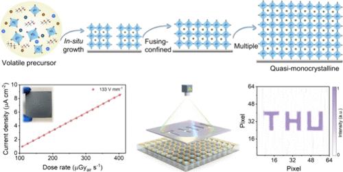
金属卤化物过氧化物因其出色的光电特性和高 X 射线衰减能力,在 X 射线探测领域大有可为。然而,制造用于高性能过氧化物 X 射线探测的大面积厚膜仍然具有挑战性。本研究开发了一种原位晶体生长和熔融约束方法,用于制备高质量、大面积的透辉石准单晶厚结晶。使用 2-甲氧基乙醇中的高浓度包晶胶体溶液原位生长包晶晶体。在原位生长和熔融约束过程中,引入甲基氯化铵可增强晶粒重组,有效减少晶界和表面缺陷。这样就能制备出结晶度高、取向均匀、垂直穿透整个薄膜厚度的大晶粒(100 微米)准单晶厚结晶。此外,厚结的载流子迁移率和寿命也显著提高。优化后的 MAPbI3 探测器的 X 射线灵敏度为 2.6 × 10⁴ μC Gyair-1 cm-2,探测极限极低,仅为 1 nGyair s-1。此外,受蜂巢结构的启发,这些探测器通过像素化分离设计实现了 64 × 64 像素的 X 射线成像,有效降低了电荷共享效应。这项研究为制备用于高灵敏 X 射线探测和成像应用的大规模过氧化物准单晶厚结提供了宝贵的见解。
In Situ Crystal Growth and Fusing-Confined Engineering of Quasi-Monocrystalline Perovskite Thick Junctions for X-ray Detection and Imaging
Metal halide perovskites exhibit great promise for utilization in X-ray detection owing to their excellent optoelectronic properties and high X-ray attenuation capabilities. However, fabricating large-area thick films for high-performance perovskite X-ray detection remains challenging. This study develops an in situ crystal growth and fusing-confined approach to prepare high-quality, large-scale perovskite quasi-monocrystalline thick junctions. The perovskite crystals are grown in situ using a highly concentrated perovskite colloidal solution in 2-methoxyethanol. Introducing methylammonium chloride enhances grain reorganization during in situ growth and fusing-confined processes, effectively reducing grain boundaries and surface defects. This allows for the preparation of quasi-monocrystalline thick junctions of large grains (>100 μm) with high crystallinity, uniform orientation, and vertical penetration across the film thickness. Additionally, the carrier mobility and lifetime of the thick junctions are significantly enhanced. The optimized MAPbI3 detectors demonstrate an X-ray sensitivity of 2.6 × 10⁴ μC Gyair–1 cm–2 and an exceptionally low detection limit of 1 nGyair s–1. Furthermore, inspired by a honeycomb structure, these detectors realize X-ray imaging in 64 × 64 pixels through a pixelated separation design, effectively reducing the charge-sharing effect. This study offers valuable insights into the preparation of large-scale perovskite quasi-monocrystalline thick junctions for highly sensitive X-ray detection and imaging applications.
期刊介绍:
ACS Nano, published monthly, serves as an international forum for comprehensive articles on nanoscience and nanotechnology research at the intersections of chemistry, biology, materials science, physics, and engineering. The journal fosters communication among scientists in these communities, facilitating collaboration, new research opportunities, and advancements through discoveries. ACS Nano covers synthesis, assembly, characterization, theory, and simulation of nanostructures, nanobiotechnology, nanofabrication, methods and tools for nanoscience and nanotechnology, and self- and directed-assembly. Alongside original research articles, it offers thorough reviews, perspectives on cutting-edge research, and discussions envisioning the future of nanoscience and nanotechnology.

 求助内容:
求助内容: 应助结果提醒方式:


