边界陷阱增强型 Ga2O3 非易失性光电存储器

IF 9.6 1区 材料科学 Q1 CHEMISTRY, MULTIDISCIPLINARY
Yonghui Zhang, Rui Zhu, Wenxing Huo, Huili Liang, Zengxia Mei
{"title":"边界陷阱增强型 Ga2O3 非易失性光电存储器","authors":"Yonghui Zhang, Rui Zhu, Wenxing Huo, Huili Liang, Zengxia Mei","doi":"10.1021/acs.nanolett.4c04235","DOIUrl":null,"url":null,"abstract":"Nonvolatile deep ultraviolet optoelectronic memory (DUVOEM) holds immense potential in cyberphysical systems, offering high storage density, swift conversion speeds, and robust data security. However, the current data retention time, typically limited to milliseconds or hours, mostly underperforms the expectations of years as a nonvolatile memory. In this work, we present a β-Ga<sub>2</sub>O<sub>3</sub>/SiO<sub>2</sub>/Si thin-film transistor DUVOEM with an enhanced data storage capability via trapping and releasing of photogenerated holes in border traps. Specifically, the photogenerated holes in β-Ga<sub>2</sub>O<sub>3</sub> will tunnel through SiO<sub>2</sub> and be captured by these defects. Innovatively, the much slower holes’ release process from the border traps has been harnessed in developing outstanding nonvolatile optoelectronic memories. Rapid writing and erasing speeds, long-time retention (≥10 years), and high robustness demonstrate its practical application values. This study not only provides a novel strategy for nonvolatile DUVOEM but also provides an instance of functionalizing β-Ga<sub>2</sub>O<sub>3</sub> memory with common defects in Si technology.","PeriodicalId":53,"journal":{"name":"Nano Letters","volume":"44 1","pages":""},"PeriodicalIF":9.6000,"publicationDate":"2024-10-30","publicationTypes":"Journal Article","fieldsOfStudy":null,"isOpenAccess":false,"openAccessPdf":"","citationCount":"0","resultStr":"{\"title\":\"Border Trap-Enhanced Ga2O3 Nonvolatile Optoelectronic Memory\",\"authors\":\"Yonghui Zhang, Rui Zhu, Wenxing Huo, Huili Liang, Zengxia Mei\",\"doi\":\"10.1021/acs.nanolett.4c04235\",\"DOIUrl\":null,\"url\":null,\"abstract\":\"Nonvolatile deep ultraviolet optoelectronic memory (DUVOEM) holds immense potential in cyberphysical systems, offering high storage density, swift conversion speeds, and robust data security. However, the current data retention time, typically limited to milliseconds or hours, mostly underperforms the expectations of years as a nonvolatile memory. In this work, we present a β-Ga<sub>2</sub>O<sub>3</sub>/SiO<sub>2</sub>/Si thin-film transistor DUVOEM with an enhanced data storage capability via trapping and releasing of photogenerated holes in border traps. Specifically, the photogenerated holes in β-Ga<sub>2</sub>O<sub>3</sub> will tunnel through SiO<sub>2</sub> and be captured by these defects. Innovatively, the much slower holes’ release process from the border traps has been harnessed in developing outstanding nonvolatile optoelectronic memories. Rapid writing and erasing speeds, long-time retention (≥10 years), and high robustness demonstrate its practical application values. This study not only provides a novel strategy for nonvolatile DUVOEM but also provides an instance of functionalizing β-Ga<sub>2</sub>O<sub>3</sub> memory with common defects in Si technology.\",\"PeriodicalId\":53,\"journal\":{\"name\":\"Nano Letters\",\"volume\":\"44 1\",\"pages\":\"\"},\"PeriodicalIF\":9.6000,\"publicationDate\":\"2024-10-30\",\"publicationTypes\":\"Journal Article\",\"fieldsOfStudy\":null,\"isOpenAccess\":false,\"openAccessPdf\":\"\",\"citationCount\":\"0\",\"resultStr\":null,\"platform\":\"Semanticscholar\",\"paperid\":null,\"PeriodicalName\":\"Nano Letters\",\"FirstCategoryId\":\"88\",\"ListUrlMain\":\"https://doi.org/10.1021/acs.nanolett.4c04235\",\"RegionNum\":1,\"RegionCategory\":\"材料科学\",\"ArticlePicture\":[],\"TitleCN\":null,\"AbstractTextCN\":null,\"PMCID\":null,\"EPubDate\":\"\",\"PubModel\":\"\",\"JCR\":\"Q1\",\"JCRName\":\"CHEMISTRY, MULTIDISCIPLINARY\",\"Score\":null,\"Total\":0}","platform":"Semanticscholar","paperid":null,"PeriodicalName":"Nano Letters","FirstCategoryId":"88","ListUrlMain":"https://doi.org/10.1021/acs.nanolett.4c04235","RegionNum":1,"RegionCategory":"材料科学","ArticlePicture":[],"TitleCN":null,"AbstractTextCN":null,"PMCID":null,"EPubDate":"","PubModel":"","JCR":"Q1","JCRName":"CHEMISTRY, MULTIDISCIPLINARY","Score":null,"Total":0}
引用次数: 0

摘要

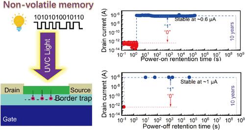
非易失性深紫外光电子存储器(DUVOEM)具有存储密度高、转换速度快和数据安全性强等特点,在网络物理系统中具有巨大的潜力。然而,目前的数据保留时间通常仅限于几毫秒或几小时,大多达不到非易失性存储器的预期年限。在这项研究中,我们提出了一种 β-Ga2O3/SiO2/Si 薄膜晶体管 DUVOEM,它通过在边界陷阱中捕获和释放光生空穴来增强数据存储能力。具体来说,β-Ga2O3 中光生成的空穴将穿过二氧化硅,并被这些缺陷捕获。创新性地利用边界陷阱中慢得多的空穴释放过程,开发出了出色的非易失性光电存储器。快速写入和擦除、长时间保留(≥10 年)和高稳健性都证明了它的实际应用价值。这项研究不仅为非易失性 DUVOEM 提供了一种新的策略,还为利用硅技术中的常见缺陷对 β-Ga2O3 存储器进行功能化提供了一个实例。
本文章由计算机程序翻译,如有差异,请以英文原文为准。

Border Trap-Enhanced Ga2O3 Nonvolatile Optoelectronic Memory

Border Trap-Enhanced Ga2O3 Nonvolatile Optoelectronic Memory
Nonvolatile deep ultraviolet optoelectronic memory (DUVOEM) holds immense potential in cyberphysical systems, offering high storage density, swift conversion speeds, and robust data security. However, the current data retention time, typically limited to milliseconds or hours, mostly underperforms the expectations of years as a nonvolatile memory. In this work, we present a β-Ga2O3/SiO2/Si thin-film transistor DUVOEM with an enhanced data storage capability via trapping and releasing of photogenerated holes in border traps. Specifically, the photogenerated holes in β-Ga2O3 will tunnel through SiO2 and be captured by these defects. Innovatively, the much slower holes’ release process from the border traps has been harnessed in developing outstanding nonvolatile optoelectronic memories. Rapid writing and erasing speeds, long-time retention (≥10 years), and high robustness demonstrate its practical application values. This study not only provides a novel strategy for nonvolatile DUVOEM but also provides an instance of functionalizing β-Ga2O3 memory with common defects in Si technology.
求助全文
通过发布文献求助,成功后即可免费获取论文全文。 去求助
来源期刊
Nano Letters
Nano Letters 工程技术-材料科学:综合
CiteScore
16.80
自引率
2.80%
发文量
1182
审稿时长
1.4 months
期刊介绍: Nano Letters serves as a dynamic platform for promptly disseminating original results in fundamental, applied, and emerging research across all facets of nanoscience and nanotechnology. A pivotal criterion for inclusion within Nano Letters is the convergence of at least two different areas or disciplines, ensuring a rich interdisciplinary scope. The journal is dedicated to fostering exploration in diverse areas, including: - Experimental and theoretical findings on physical, chemical, and biological phenomena at the nanoscale - Synthesis, characterization, and processing of organic, inorganic, polymer, and hybrid nanomaterials through physical, chemical, and biological methodologies - Modeling and simulation of synthetic, assembly, and interaction processes - Realization of integrated nanostructures and nano-engineered devices exhibiting advanced performance - Applications of nanoscale materials in living and environmental systems Nano Letters is committed to advancing and showcasing groundbreaking research that intersects various domains, fostering innovation and collaboration in the ever-evolving field of nanoscience and nanotechnology.
×
引用
GB/T 7714-2015
复制
MLA
复制
APA
复制
导出至
BibTeX EndNote RefMan NoteFirst NoteExpress
×
提示
您的信息不完整,为了账户安全,请先补充。
现在去补充
×
提示
您因"违规操作"
具体请查看互助需知
我知道了
×
提示
确定
请完成安全验证×
copy
已复制链接
快去分享给好友吧!
我知道了
右上角分享
点击右上角分享
0
联系我们:info@booksci.cn Book学术提供免费学术资源搜索服务,方便国内外学者检索中英文文献。致力于提供最便捷和优质的服务体验。 Copyright © 2023 布克学术 All rights reserved.
京ICP备2023020795号-1
ghs 京公网安备 11010802042870号
Book学术文献互助
Book学术文献互助群
群 号:481959085
Book学术官方微信