{"title":"通过电化学蚀刻和反应性直流溅射制备的氮化钒/多孔硅异质结光电探测器的光电性能提升","authors":"","doi":"10.1016/j.jics.2024.101432","DOIUrl":null,"url":null,"abstract":"<div><div>In this work, vanadium nitride (VN) thin films were deposited on porous silicon using the DC sputtering technique. The porous silicon was prepared using the electrochemical etching method at various current densities. X-ray diffraction (XRD), field emission scanning electron microscopy (FE-SEM), Fourier transform infrared (FTIR) spectroscopy, UV–visible spectrometry, and photoluminescence (PL) spectroscopy were used to study the structural, morphological, chemical, and optical characteristics of the vanadium nitride and porous silicon. X-ray diffraction studies showed that the deposited vanadium nitride film was crystalline in nature with a cubic structure. The VN particles were found to be embedded inside the pores of the porous silicon. The crystallite size of the VN film was 8 nm. The optical absorption results showed that the optical energy gap of vanadium nitride was 2.98 eV. The photoluminescence spectra revealed the presence of four emission peaks located at 441, 496, 541, and 720 nm. The electrical properties of the VN/PSi heterojunction, including dark and illuminated current-voltage characteristics as a function of etching current density, were investigated. The best ideality factor was 3.1 for heterojunction prepared at a current density of 8 mA/cm<sup>2</sup>. A responsivity of 3.7 A/W and a detectivity of 6.5 × 10<sup>11</sup> Jones at 500 nm were found for the photodetector fabricated at a current density of 8 mA/cm<sup>2</sup>. The (I-t) response of the photodetectors were determined.</div></div>","PeriodicalId":17276,"journal":{"name":"Journal of the Indian Chemical Society","volume":null,"pages":null},"PeriodicalIF":3.2000,"publicationDate":"2024-10-18","publicationTypes":"Journal Article","fieldsOfStudy":null,"isOpenAccess":false,"openAccessPdf":"","citationCount":"0","resultStr":"{\"title\":\"Enhancement of optoelectronic properties of Vanadium nitride/porous silicon heterojunction photodetector prepared by electrochemical etching and reactive DC sputtering\",\"authors\":\"\",\"doi\":\"10.1016/j.jics.2024.101432\",\"DOIUrl\":null,\"url\":null,\"abstract\":\"<div><div>In this work, vanadium nitride (VN) thin films were deposited on porous silicon using the DC sputtering technique. The porous silicon was prepared using the electrochemical etching method at various current densities. X-ray diffraction (XRD), field emission scanning electron microscopy (FE-SEM), Fourier transform infrared (FTIR) spectroscopy, UV–visible spectrometry, and photoluminescence (PL) spectroscopy were used to study the structural, morphological, chemical, and optical characteristics of the vanadium nitride and porous silicon. X-ray diffraction studies showed that the deposited vanadium nitride film was crystalline in nature with a cubic structure. The VN particles were found to be embedded inside the pores of the porous silicon. The crystallite size of the VN film was 8 nm. The optical absorption results showed that the optical energy gap of vanadium nitride was 2.98 eV. The photoluminescence spectra revealed the presence of four emission peaks located at 441, 496, 541, and 720 nm. The electrical properties of the VN/PSi heterojunction, including dark and illuminated current-voltage characteristics as a function of etching current density, were investigated. The best ideality factor was 3.1 for heterojunction prepared at a current density of 8 mA/cm<sup>2</sup>. A responsivity of 3.7 A/W and a detectivity of 6.5 × 10<sup>11</sup> Jones at 500 nm were found for the photodetector fabricated at a current density of 8 mA/cm<sup>2</sup>. The (I-t) response of the photodetectors were determined.</div></div>\",\"PeriodicalId\":17276,\"journal\":{\"name\":\"Journal of the Indian Chemical Society\",\"volume\":null,\"pages\":null},\"PeriodicalIF\":3.2000,\"publicationDate\":\"2024-10-18\",\"publicationTypes\":\"Journal Article\",\"fieldsOfStudy\":null,\"isOpenAccess\":false,\"openAccessPdf\":\"\",\"citationCount\":\"0\",\"resultStr\":null,\"platform\":\"Semanticscholar\",\"paperid\":null,\"PeriodicalName\":\"Journal of the Indian Chemical Society\",\"FirstCategoryId\":\"92\",\"ListUrlMain\":\"https://www.sciencedirect.com/science/article/pii/S0019452224003121\",\"RegionNum\":4,\"RegionCategory\":\"化学\",\"ArticlePicture\":[],\"TitleCN\":null,\"AbstractTextCN\":null,\"PMCID\":null,\"EPubDate\":\"\",\"PubModel\":\"\",\"JCR\":\"Q2\",\"JCRName\":\"CHEMISTRY, MULTIDISCIPLINARY\",\"Score\":null,\"Total\":0}","platform":"Semanticscholar","paperid":null,"PeriodicalName":"Journal of the Indian Chemical Society","FirstCategoryId":"92","ListUrlMain":"https://www.sciencedirect.com/science/article/pii/S0019452224003121","RegionNum":4,"RegionCategory":"化学","ArticlePicture":[],"TitleCN":null,"AbstractTextCN":null,"PMCID":null,"EPubDate":"","PubModel":"","JCR":"Q2","JCRName":"CHEMISTRY, MULTIDISCIPLINARY","Score":null,"Total":0}
Enhancement of optoelectronic properties of Vanadium nitride/porous silicon heterojunction photodetector prepared by electrochemical etching and reactive DC sputtering
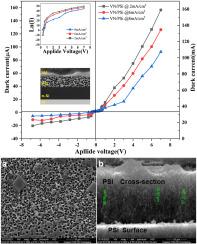
In this work, vanadium nitride (VN) thin films were deposited on porous silicon using the DC sputtering technique. The porous silicon was prepared using the electrochemical etching method at various current densities. X-ray diffraction (XRD), field emission scanning electron microscopy (FE-SEM), Fourier transform infrared (FTIR) spectroscopy, UV–visible spectrometry, and photoluminescence (PL) spectroscopy were used to study the structural, morphological, chemical, and optical characteristics of the vanadium nitride and porous silicon. X-ray diffraction studies showed that the deposited vanadium nitride film was crystalline in nature with a cubic structure. The VN particles were found to be embedded inside the pores of the porous silicon. The crystallite size of the VN film was 8 nm. The optical absorption results showed that the optical energy gap of vanadium nitride was 2.98 eV. The photoluminescence spectra revealed the presence of four emission peaks located at 441, 496, 541, and 720 nm. The electrical properties of the VN/PSi heterojunction, including dark and illuminated current-voltage characteristics as a function of etching current density, were investigated. The best ideality factor was 3.1 for heterojunction prepared at a current density of 8 mA/cm2. A responsivity of 3.7 A/W and a detectivity of 6.5 × 10¹¹ Jones at 500 nm were found for the photodetector fabricated at a current density of 8 mA/cm2. The (I-t) response of the photodetectors were determined.
期刊介绍:
The Journal of the Indian Chemical Society publishes original, fundamental, theorical, experimental research work of highest quality in all areas of chemistry, biochemistry, medicinal chemistry, electrochemistry, agrochemistry, chemical engineering and technology, food chemistry, environmental chemistry, etc.