通过原位种子层带隙工程实现传导带偏移恢复和具有高开路电压的高效 Sb2Se3 太阳能电池

IF 13.1 1区 化学 Q1 Energy
{"title":"通过原位种子层带隙工程实现传导带偏移恢复和具有高开路电压的高效 Sb2Se3 太阳能电池","authors":"","doi":"10.1016/j.jechem.2024.09.042","DOIUrl":null,"url":null,"abstract":"<div><div>Sb<sub>2</sub>Se<sub>3</sub> solar cells have achieved a power conversion efficiency (PCE) of over 10%. However, the serious open-circuit voltage deficit (<em>V</em><sub>OC</sub>-deficit), induced by the hard-to-control crystal orientation and heterojunction interface reaction, limits the PCE of vapor transport deposition (VTD) processed Sb<sub>2</sub>Se<sub>3</sub> solar cells. To overcome the <em>V</em><sub>OC</sub>-deficit problem of VTD processed Sb<sub>2</sub>Se<sub>3</sub> solar cells, herein, an in-situ bandgap regulation strategy is innovatively proposed to prepare a wide band gap Sb<sub>2</sub>(S,Se)<sub>3</sub> seed layer (WBSL) at CdS/Sb<sub>2</sub>Se<sub>3</sub> heterojunction interface to improve the PCE of Sb<sub>2</sub>Se<sub>3</sub> solar cells. The analysis results show that the introduced Sb<sub>2</sub>(S,Se)<sub>3</sub> seed layer can enhance the [001] orientation of Sb<sub>2</sub>Se<sub>3</sub> thin films, broaden the band gap of heterojunction interface, and realize a “Spike-like” conduction band alignment with Δ<em>E</em><sub>c</sub> = 0.11 eV. In addition, thanks to the suppressed CdS/Sb<sub>2</sub>Se<sub>3</sub> interface reaction after WBSL application, the depletion region width of Sb<sub>2</sub>Se<sub>3</sub> solar cells is widened, and the quality of CdS/Sb<sub>2</sub>Se<sub>3</sub> interface and the carrier transporting performance of Sb<sub>2</sub>Se<sub>3</sub> solar cells are significantly improved as well. Moreover, the harmful Se vacancy defects near the front interface of Sb<sub>2</sub>Se<sub>3</sub> solar cells can be greatly diminished by WBSL. Finally, the PCE of Sb<sub>2</sub>Se<sub>3</sub> solar cells is improved from 7.0% to 7.6%; meanwhile the <em>V</em><sub>OC</sub> is increased to 466 mV which is the highest value for the VTD derived Sb<sub>2</sub>Se<sub>3</sub> solar cells. This work will provide a valuable reference for the interface and orientation regulation of antimony-based chalcogenide solar cells.</div></div>","PeriodicalId":15728,"journal":{"name":"Journal of Energy Chemistry","volume":null,"pages":null},"PeriodicalIF":13.1000,"publicationDate":"2024-10-02","publicationTypes":"Journal Article","fieldsOfStudy":null,"isOpenAccess":false,"openAccessPdf":"","citationCount":"0","resultStr":"{\"title\":\"In situ seed layer bandgap engineering leading to the conduction band offset reversion and efficient Sb2Se3 solar cells with high open-circuit voltage\",\"authors\":\"\",\"doi\":\"10.1016/j.jechem.2024.09.042\",\"DOIUrl\":null,\"url\":null,\"abstract\":\"<div><div>Sb<sub>2</sub>Se<sub>3</sub> solar cells have achieved a power conversion efficiency (PCE) of over 10%. However, the serious open-circuit voltage deficit (<em>V</em><sub>OC</sub>-deficit), induced by the hard-to-control crystal orientation and heterojunction interface reaction, limits the PCE of vapor transport deposition (VTD) processed Sb<sub>2</sub>Se<sub>3</sub> solar cells. To overcome the <em>V</em><sub>OC</sub>-deficit problem of VTD processed Sb<sub>2</sub>Se<sub>3</sub> solar cells, herein, an in-situ bandgap regulation strategy is innovatively proposed to prepare a wide band gap Sb<sub>2</sub>(S,Se)<sub>3</sub> seed layer (WBSL) at CdS/Sb<sub>2</sub>Se<sub>3</sub> heterojunction interface to improve the PCE of Sb<sub>2</sub>Se<sub>3</sub> solar cells. The analysis results show that the introduced Sb<sub>2</sub>(S,Se)<sub>3</sub> seed layer can enhance the [001] orientation of Sb<sub>2</sub>Se<sub>3</sub> thin films, broaden the band gap of heterojunction interface, and realize a “Spike-like” conduction band alignment with Δ<em>E</em><sub>c</sub> = 0.11 eV. In addition, thanks to the suppressed CdS/Sb<sub>2</sub>Se<sub>3</sub> interface reaction after WBSL application, the depletion region width of Sb<sub>2</sub>Se<sub>3</sub> solar cells is widened, and the quality of CdS/Sb<sub>2</sub>Se<sub>3</sub> interface and the carrier transporting performance of Sb<sub>2</sub>Se<sub>3</sub> solar cells are significantly improved as well. Moreover, the harmful Se vacancy defects near the front interface of Sb<sub>2</sub>Se<sub>3</sub> solar cells can be greatly diminished by WBSL. Finally, the PCE of Sb<sub>2</sub>Se<sub>3</sub> solar cells is improved from 7.0% to 7.6%; meanwhile the <em>V</em><sub>OC</sub> is increased to 466 mV which is the highest value for the VTD derived Sb<sub>2</sub>Se<sub>3</sub> solar cells. This work will provide a valuable reference for the interface and orientation regulation of antimony-based chalcogenide solar cells.</div></div>\",\"PeriodicalId\":15728,\"journal\":{\"name\":\"Journal of Energy Chemistry\",\"volume\":null,\"pages\":null},\"PeriodicalIF\":13.1000,\"publicationDate\":\"2024-10-02\",\"publicationTypes\":\"Journal Article\",\"fieldsOfStudy\":null,\"isOpenAccess\":false,\"openAccessPdf\":\"\",\"citationCount\":\"0\",\"resultStr\":null,\"platform\":\"Semanticscholar\",\"paperid\":null,\"PeriodicalName\":\"Journal of Energy Chemistry\",\"FirstCategoryId\":\"92\",\"ListUrlMain\":\"https://www.sciencedirect.com/science/article/pii/S2095495624006661\",\"RegionNum\":1,\"RegionCategory\":\"化学\",\"ArticlePicture\":[],\"TitleCN\":null,\"AbstractTextCN\":null,\"PMCID\":null,\"EPubDate\":\"\",\"PubModel\":\"\",\"JCR\":\"Q1\",\"JCRName\":\"Energy\",\"Score\":null,\"Total\":0}","platform":"Semanticscholar","paperid":null,"PeriodicalName":"Journal of Energy Chemistry","FirstCategoryId":"92","ListUrlMain":"https://www.sciencedirect.com/science/article/pii/S2095495624006661","RegionNum":1,"RegionCategory":"化学","ArticlePicture":[],"TitleCN":null,"AbstractTextCN":null,"PMCID":null,"EPubDate":"","PubModel":"","JCR":"Q1","JCRName":"Energy","Score":null,"Total":0}
引用次数: 0

摘要

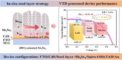
Sb2Se3 太阳能电池的功率转换效率(PCE)已超过 10%。然而,难以控制的晶体取向和异质结界面反应导致的严重开路电压不足(VOC-deficit)限制了气相传输沉积(VTD)工艺 Sb2Se3 太阳能电池的 PCE。为了克服 VTD 工艺 Sb2Se3 太阳能电池的 VOC 缺陷问题,本文创新性地提出了一种原位带隙调节策略,在 CdS/Sb2Se3 异质结界面制备宽带隙 Sb2(S,Se)3 种子层 (WBSL),以提高 Sb2Se3 太阳能电池的 PCE。分析结果表明,引入的 Sb2(S,Se)3 种子层可以增强 Sb2Se3 薄膜的 [001] 取向,拓宽异质结界面的带隙,实现ΔEc = 0.11 eV 的 "穗状 "导带排列。此外,由于 WBSL 应用后抑制了 CdS/Sb2Se3 界面反应,Sb2Se3 太阳能电池的耗尽区宽度得以拓宽,CdS/Sb2Se3 界面的质量和 Sb2Se3 太阳能电池的载流子传输性能也得到了显著改善。此外,WBSL 还能大大减少 Sb2Se3 太阳能电池正面界面附近有害的 Se 空位缺陷。最后,Sb2Se3 太阳能电池的 PCE 从 7.0% 提高到 7.6%,同时 VOC 提高到 466 mV,这是 VTD 衍生 Sb2Se3 太阳能电池的最高值。这项工作将为锑基铬化镓太阳能电池的界面和取向调节提供有价值的参考。
本文章由计算机程序翻译,如有差异,请以英文原文为准。

In situ seed layer bandgap engineering leading to the conduction band offset reversion and efficient Sb2Se3 solar cells with high open-circuit voltage

In situ seed layer bandgap engineering leading to the conduction band offset reversion and efficient Sb2Se3 solar cells with high open-circuit voltage
Sb2Se3 solar cells have achieved a power conversion efficiency (PCE) of over 10%. However, the serious open-circuit voltage deficit (VOC-deficit), induced by the hard-to-control crystal orientation and heterojunction interface reaction, limits the PCE of vapor transport deposition (VTD) processed Sb2Se3 solar cells. To overcome the VOC-deficit problem of VTD processed Sb2Se3 solar cells, herein, an in-situ bandgap regulation strategy is innovatively proposed to prepare a wide band gap Sb2(S,Se)3 seed layer (WBSL) at CdS/Sb2Se3 heterojunction interface to improve the PCE of Sb2Se3 solar cells. The analysis results show that the introduced Sb2(S,Se)3 seed layer can enhance the [001] orientation of Sb2Se3 thin films, broaden the band gap of heterojunction interface, and realize a “Spike-like” conduction band alignment with ΔEc = 0.11 eV. In addition, thanks to the suppressed CdS/Sb2Se3 interface reaction after WBSL application, the depletion region width of Sb2Se3 solar cells is widened, and the quality of CdS/Sb2Se3 interface and the carrier transporting performance of Sb2Se3 solar cells are significantly improved as well. Moreover, the harmful Se vacancy defects near the front interface of Sb2Se3 solar cells can be greatly diminished by WBSL. Finally, the PCE of Sb2Se3 solar cells is improved from 7.0% to 7.6%; meanwhile the VOC is increased to 466 mV which is the highest value for the VTD derived Sb2Se3 solar cells. This work will provide a valuable reference for the interface and orientation regulation of antimony-based chalcogenide solar cells.
求助全文
通过发布文献求助,成功后即可免费获取论文全文。 去求助
来源期刊
Journal of Energy Chemistry
Journal of Energy Chemistry CHEMISTRY, APPLIED-CHEMISTRY, PHYSICAL
CiteScore
19.10
自引率
8.40%
发文量
3631
审稿时长
15 days
期刊介绍: The Journal of Energy Chemistry, the official publication of Science Press and the Dalian Institute of Chemical Physics, Chinese Academy of Sciences, serves as a platform for reporting creative research and innovative applications in energy chemistry. It mainly reports on creative researches and innovative applications of chemical conversions of fossil energy, carbon dioxide, electrochemical energy and hydrogen energy, as well as the conversions of biomass and solar energy related with chemical issues to promote academic exchanges in the field of energy chemistry and to accelerate the exploration, research and development of energy science and technologies. This journal focuses on original research papers covering various topics within energy chemistry worldwide, including: Optimized utilization of fossil energy Hydrogen energy Conversion and storage of electrochemical energy Capture, storage, and chemical conversion of carbon dioxide Materials and nanotechnologies for energy conversion and storage Chemistry in biomass conversion Chemistry in the utilization of solar energy
×
引用
GB/T 7714-2015
复制
MLA
复制
APA
复制
导出至
BibTeX EndNote RefMan NoteFirst NoteExpress
×
提示
您的信息不完整,为了账户安全,请先补充。
现在去补充
×
提示
您因"违规操作"
具体请查看互助需知
我知道了
×
提示
确定
请完成安全验证×
copy
已复制链接
快去分享给好友吧!
我知道了
右上角分享
点击右上角分享
0
联系我们:info@booksci.cn Book学术提供免费学术资源搜索服务,方便国内外学者检索中英文文献。致力于提供最便捷和优质的服务体验。 Copyright © 2023 布克学术 All rights reserved.
京ICP备2023020795号-1
ghs 京公网安备 11010802042870号
Book学术文献互助
Book学术文献互助群
群 号:481959085
Book学术官方微信