Suprovat Ghosh, Abir Mukherjee, Sudarshan Singh, Samit K Ray, Ananjan Basu, Santanu Manna and Samaresh Das*,
{"title":"通过分子束外延生长的 II 型 Ge QD/Si 异质结构中的光泵浦太赫兹振幅调制","authors":"Suprovat Ghosh, Abir Mukherjee, Sudarshan Singh, Samit K Ray, Ananjan Basu, Santanu Manna and Samaresh Das*, ","doi":"10.1021/acsaom.4c0029810.1021/acsaom.4c00298","DOIUrl":null,"url":null,"abstract":"<p >This article explores group-IV germanium (Ge) quantum dots (QDs) on silicon-on-insulator (SOI) grown by molecular beam epitaxy (MBE) in order to explore their optical behavior in the terahertz (THz) regime. In this work, Ge QDs, pumped by an above bandgap near–infrared wavelength, exhibit THz amplitude modulation in the frequency range of 0.1–1.0 THz. The epitaxial Ge QDs outperform the reference SOI (170 nm top Si) substrate in THz amplitude modulation due to higher carrier generation in weakly confined dots compared to their bulk counterpart. This is further corroborated using a theoretical model based on the nonequilibrium Green’s function (NEGF) method. This model enables the calculation of photocarrier generated (PCG) and their confinement in the Ge QD region. Our model also reroutes the calculation from PCG to the corresponding plasma frequency and hence to refractive index and THz photoconductivity. Moreover, the photogenerated confined holes’ accumulation at the Ge QDs/Si interface is elevated after optical illumination, leading to decreased THz photoconductivity. This augmentation in THz photoconductivity contributes to a significant enhancement of THz modulation depth of ∼77% at Ge QDs/Si interfaces compared to bare SOI at 0.1 THz.</p>","PeriodicalId":29803,"journal":{"name":"ACS Applied Optical Materials","volume":"2 10","pages":"2085–2091 2085–2091"},"PeriodicalIF":0.0000,"publicationDate":"2024-10-03","publicationTypes":"Journal Article","fieldsOfStudy":null,"isOpenAccess":false,"openAccessPdf":"","citationCount":"0","resultStr":"{\"title\":\"Optically Pumped Terahertz Amplitude Modulation in Type-II Ge QD/Si Heterostructures Grown via Molecular Beam Epitaxy\",\"authors\":\"Suprovat Ghosh, Abir Mukherjee, Sudarshan Singh, Samit K Ray, Ananjan Basu, Santanu Manna and Samaresh Das*, \",\"doi\":\"10.1021/acsaom.4c0029810.1021/acsaom.4c00298\",\"DOIUrl\":null,\"url\":null,\"abstract\":\"<p >This article explores group-IV germanium (Ge) quantum dots (QDs) on silicon-on-insulator (SOI) grown by molecular beam epitaxy (MBE) in order to explore their optical behavior in the terahertz (THz) regime. In this work, Ge QDs, pumped by an above bandgap near–infrared wavelength, exhibit THz amplitude modulation in the frequency range of 0.1–1.0 THz. The epitaxial Ge QDs outperform the reference SOI (170 nm top Si) substrate in THz amplitude modulation due to higher carrier generation in weakly confined dots compared to their bulk counterpart. This is further corroborated using a theoretical model based on the nonequilibrium Green’s function (NEGF) method. This model enables the calculation of photocarrier generated (PCG) and their confinement in the Ge QD region. Our model also reroutes the calculation from PCG to the corresponding plasma frequency and hence to refractive index and THz photoconductivity. Moreover, the photogenerated confined holes’ accumulation at the Ge QDs/Si interface is elevated after optical illumination, leading to decreased THz photoconductivity. This augmentation in THz photoconductivity contributes to a significant enhancement of THz modulation depth of ∼77% at Ge QDs/Si interfaces compared to bare SOI at 0.1 THz.</p>\",\"PeriodicalId\":29803,\"journal\":{\"name\":\"ACS Applied Optical Materials\",\"volume\":\"2 10\",\"pages\":\"2085–2091 2085–2091\"},\"PeriodicalIF\":0.0000,\"publicationDate\":\"2024-10-03\",\"publicationTypes\":\"Journal Article\",\"fieldsOfStudy\":null,\"isOpenAccess\":false,\"openAccessPdf\":\"\",\"citationCount\":\"0\",\"resultStr\":null,\"platform\":\"Semanticscholar\",\"paperid\":null,\"PeriodicalName\":\"ACS Applied Optical Materials\",\"FirstCategoryId\":\"1085\",\"ListUrlMain\":\"https://pubs.acs.org/doi/10.1021/acsaom.4c00298\",\"RegionNum\":0,\"RegionCategory\":null,\"ArticlePicture\":[],\"TitleCN\":null,\"AbstractTextCN\":null,\"PMCID\":null,\"EPubDate\":\"\",\"PubModel\":\"\",\"JCR\":\"\",\"JCRName\":\"\",\"Score\":null,\"Total\":0}","platform":"Semanticscholar","paperid":null,"PeriodicalName":"ACS Applied Optical Materials","FirstCategoryId":"1085","ListUrlMain":"https://pubs.acs.org/doi/10.1021/acsaom.4c00298","RegionNum":0,"RegionCategory":null,"ArticlePicture":[],"TitleCN":null,"AbstractTextCN":null,"PMCID":null,"EPubDate":"","PubModel":"","JCR":"","JCRName":"","Score":null,"Total":0}
引用次数: 0
摘要
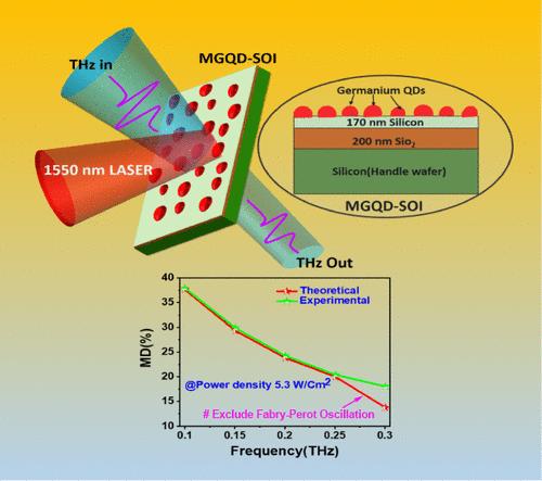
本文探讨了分子束外延(MBE)技术在硅绝缘体(SOI)上生长的第四族锗(Ge)量子点(QDs),以探索它们在太赫兹(THz)机制下的光学行为。在这项研究中,Ge QD 在高于带隙的近红外波长的泵浦作用下,在 0.1-1.0 太赫兹的频率范围内表现出太赫兹振幅调制。外延 Ge QD 在太赫兹振幅调制方面优于参考 SOI(170 nm 顶部硅)衬底,这是由于弱约束点中的载流子生成量高于其块状对应物。基于非平衡格林函数 (NEGF) 方法的理论模型进一步证实了这一点。该模型能够计算产生的光载流子(PCG)及其在 Ge QD 区域的约束。我们的模型还将计算从 PCG 转向相应的等离子体频率,进而转向折射率和太赫兹光电导率。此外,在光照之后,Ge QDs/Si 界面上光生成的封闭空穴堆积会增加,从而导致太赫兹光电导率降低。太赫兹光导率的提高使 Ge QDs/Si 界面的太赫兹调制深度在 0.1 太赫兹时比裸 SOI 界面显著提高了 ∼ 77%。
Optically Pumped Terahertz Amplitude Modulation in Type-II Ge QD/Si Heterostructures Grown via Molecular Beam Epitaxy
This article explores group-IV germanium (Ge) quantum dots (QDs) on silicon-on-insulator (SOI) grown by molecular beam epitaxy (MBE) in order to explore their optical behavior in the terahertz (THz) regime. In this work, Ge QDs, pumped by an above bandgap near–infrared wavelength, exhibit THz amplitude modulation in the frequency range of 0.1–1.0 THz. The epitaxial Ge QDs outperform the reference SOI (170 nm top Si) substrate in THz amplitude modulation due to higher carrier generation in weakly confined dots compared to their bulk counterpart. This is further corroborated using a theoretical model based on the nonequilibrium Green’s function (NEGF) method. This model enables the calculation of photocarrier generated (PCG) and their confinement in the Ge QD region. Our model also reroutes the calculation from PCG to the corresponding plasma frequency and hence to refractive index and THz photoconductivity. Moreover, the photogenerated confined holes’ accumulation at the Ge QDs/Si interface is elevated after optical illumination, leading to decreased THz photoconductivity. This augmentation in THz photoconductivity contributes to a significant enhancement of THz modulation depth of ∼77% at Ge QDs/Si interfaces compared to bare SOI at 0.1 THz.
期刊介绍:
ACS Applied Optical Materials is an international and interdisciplinary forum to publish original experimental and theoretical including simulation and modeling research in optical materials complementing the ACS Applied Materials portfolio. With a focus on innovative applications ACS Applied Optical Materials also complements and expands the scope of existing ACS publications that focus on fundamental aspects of the interaction between light and matter in materials science including ACS Photonics Macromolecules Journal of Physical Chemistry C ACS Nano and Nano Letters.The scope of ACS Applied Optical Materials includes high quality research of an applied nature that integrates knowledge in materials science chemistry physics optical science and engineering.
 求助内容:
求助内容: 应助结果提醒方式:


