Marc Jaikissoon, Çağıl Köroğlu, Jerry A. Yang, Kathryn Neilson, Krishna C. Saraswat, Eric Pop
{"title":"单层半导体晶体管的 CMOS 兼容应变工程","authors":"Marc Jaikissoon, Çağıl Köroğlu, Jerry A. Yang, Kathryn Neilson, Krishna C. Saraswat, Eric Pop","doi":"10.1038/s41928-024-01244-7","DOIUrl":null,"url":null,"abstract":"Strain engineering has played a key role in modern silicon electronics, having been introduced as a mobility booster in the 1990s and commercialized in the early 2000s. Achieving similar advances with two-dimensional (2D) semiconductors in a complementary metal–oxide–semiconductor (CMOS)-compatible manner could improve the industrial viability of 2D material transistors. Here, we show that silicon nitride capping layers can impart strain to monolayer molybdenum disulfide (MoS2) transistors on conventional silicon substrates, improving their performance with a CMOS-compatible approach, at a low thermal budget of 350 °C. Strained back-gated and dual-gated MoS2 transistors exhibit median increases in on-state current of up to 60% and 45%, respectively. The greatest improvements are found when reducing both transistor channels and contacts from micrometre-scale to 200 nm, reaching saturation currents of 488 µA µm−1 in devices with just 400 nm contact pitch. Simulations show that the performance enhancement is mainly due to tensile strain lowering the contact Schottky barriers, and that further reducing device dimensions, including contacts, could lead to additional increases in strain and performance. The on-current performance of MoS2-based transistors can be improved by using silicon nitride capping layers that apply strain to the devices.","PeriodicalId":19064,"journal":{"name":"Nature Electronics","volume":"7 10","pages":"885-891"},"PeriodicalIF":33.7000,"publicationDate":"2024-10-23","publicationTypes":"Journal Article","fieldsOfStudy":null,"isOpenAccess":false,"openAccessPdf":"","citationCount":"0","resultStr":"{\"title\":\"CMOS-compatible strain engineering for monolayer semiconductor transistors\",\"authors\":\"Marc Jaikissoon, Çağıl Köroğlu, Jerry A. Yang, Kathryn Neilson, Krishna C. Saraswat, Eric Pop\",\"doi\":\"10.1038/s41928-024-01244-7\",\"DOIUrl\":null,\"url\":null,\"abstract\":\"Strain engineering has played a key role in modern silicon electronics, having been introduced as a mobility booster in the 1990s and commercialized in the early 2000s. Achieving similar advances with two-dimensional (2D) semiconductors in a complementary metal–oxide–semiconductor (CMOS)-compatible manner could improve the industrial viability of 2D material transistors. Here, we show that silicon nitride capping layers can impart strain to monolayer molybdenum disulfide (MoS2) transistors on conventional silicon substrates, improving their performance with a CMOS-compatible approach, at a low thermal budget of 350 °C. Strained back-gated and dual-gated MoS2 transistors exhibit median increases in on-state current of up to 60% and 45%, respectively. The greatest improvements are found when reducing both transistor channels and contacts from micrometre-scale to 200 nm, reaching saturation currents of 488 µA µm−1 in devices with just 400 nm contact pitch. Simulations show that the performance enhancement is mainly due to tensile strain lowering the contact Schottky barriers, and that further reducing device dimensions, including contacts, could lead to additional increases in strain and performance. The on-current performance of MoS2-based transistors can be improved by using silicon nitride capping layers that apply strain to the devices.\",\"PeriodicalId\":19064,\"journal\":{\"name\":\"Nature Electronics\",\"volume\":\"7 10\",\"pages\":\"885-891\"},\"PeriodicalIF\":33.7000,\"publicationDate\":\"2024-10-23\",\"publicationTypes\":\"Journal Article\",\"fieldsOfStudy\":null,\"isOpenAccess\":false,\"openAccessPdf\":\"\",\"citationCount\":\"0\",\"resultStr\":null,\"platform\":\"Semanticscholar\",\"paperid\":null,\"PeriodicalName\":\"Nature Electronics\",\"FirstCategoryId\":\"5\",\"ListUrlMain\":\"https://www.nature.com/articles/s41928-024-01244-7\",\"RegionNum\":1,\"RegionCategory\":\"工程技术\",\"ArticlePicture\":[],\"TitleCN\":null,\"AbstractTextCN\":null,\"PMCID\":null,\"EPubDate\":\"\",\"PubModel\":\"\",\"JCR\":\"Q1\",\"JCRName\":\"ENGINEERING, ELECTRICAL & ELECTRONIC\",\"Score\":null,\"Total\":0}","platform":"Semanticscholar","paperid":null,"PeriodicalName":"Nature Electronics","FirstCategoryId":"5","ListUrlMain":"https://www.nature.com/articles/s41928-024-01244-7","RegionNum":1,"RegionCategory":"工程技术","ArticlePicture":[],"TitleCN":null,"AbstractTextCN":null,"PMCID":null,"EPubDate":"","PubModel":"","JCR":"Q1","JCRName":"ENGINEERING, ELECTRICAL & ELECTRONIC","Score":null,"Total":0}
CMOS-compatible strain engineering for monolayer semiconductor transistors
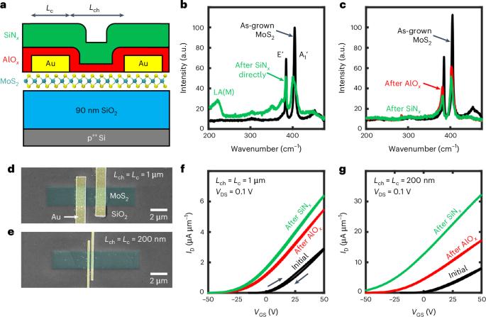
Strain engineering has played a key role in modern silicon electronics, having been introduced as a mobility booster in the 1990s and commercialized in the early 2000s. Achieving similar advances with two-dimensional (2D) semiconductors in a complementary metal–oxide–semiconductor (CMOS)-compatible manner could improve the industrial viability of 2D material transistors. Here, we show that silicon nitride capping layers can impart strain to monolayer molybdenum disulfide (MoS2) transistors on conventional silicon substrates, improving their performance with a CMOS-compatible approach, at a low thermal budget of 350 °C. Strained back-gated and dual-gated MoS2 transistors exhibit median increases in on-state current of up to 60% and 45%, respectively. The greatest improvements are found when reducing both transistor channels and contacts from micrometre-scale to 200 nm, reaching saturation currents of 488 µA µm−1 in devices with just 400 nm contact pitch. Simulations show that the performance enhancement is mainly due to tensile strain lowering the contact Schottky barriers, and that further reducing device dimensions, including contacts, could lead to additional increases in strain and performance. The on-current performance of MoS2-based transistors can be improved by using silicon nitride capping layers that apply strain to the devices.
期刊介绍:
Nature Electronics is a comprehensive journal that publishes both fundamental and applied research in the field of electronics. It encompasses a wide range of topics, including the study of new phenomena and devices, the design and construction of electronic circuits, and the practical applications of electronics. In addition, the journal explores the commercial and industrial aspects of electronics research.
The primary focus of Nature Electronics is on the development of technology and its potential impact on society. The journal incorporates the contributions of scientists, engineers, and industry professionals, offering a platform for their research findings. Moreover, Nature Electronics provides insightful commentary, thorough reviews, and analysis of the key issues that shape the field, as well as the technologies that are reshaping society.
Like all journals within the prestigious Nature brand, Nature Electronics upholds the highest standards of quality. It maintains a dedicated team of professional editors and follows a fair and rigorous peer-review process. The journal also ensures impeccable copy-editing and production, enabling swift publication. Additionally, Nature Electronics prides itself on its editorial independence, ensuring unbiased and impartial reporting.
In summary, Nature Electronics is a leading journal that publishes cutting-edge research in electronics. With its multidisciplinary approach and commitment to excellence, the journal serves as a valuable resource for scientists, engineers, and industry professionals seeking to stay at the forefront of advancements in the field.