与 λ/5000 纳米波导的定向耦合
IF 15.8
1区 材料科学
Q1 CHEMISTRY, MULTIDISCIPLINARY
引用次数: 0
摘要
硅基微型器件被认为是将几种太赫兹技术整合到一个通用实用平台的理想候选器件。其实用性源于相对较低的损耗、器件结构紧凑、易于制造以及广泛的无源和有源功能。然而,典型器件的尺寸受限于几百微米的衍射,这阻碍了太赫兹频率下新兴的纳米级应用。虽然金属间隙模式可提供纳米级太赫兹约束,但与之有效耦合却十分困难。在此,我们提出并通过实验证明了一种策略,可将亚太赫兹辐射(λ = 1 毫米)有效地连接到由金膜上蚀刻的纳米间隙形成的波导,该波导宽 200 纳米(λ/5000),长达 4.5 毫米。设计原理依赖于电介质和纳米间隙波导模式的相位匹配,当它们并排放置时,可产生有效的定向耦合。通过介质波导进行的宽带远场太赫兹传输实验显示,由于谐振耦合,在设计波长附近会出现传输衰减。在金层表面进行的近场测量证实,这种衰减伴随着功率向纳米间隙的转移,估计耦合效率为 10%。我们的方法以定制和可控的方式有效地将毫米波与纳米级波导连接起来,对片上纳米光谱学、电信和量子技术具有重要意义。本文章由计算机程序翻译,如有差异,请以英文原文为准。
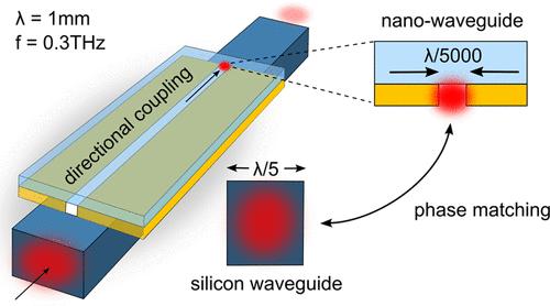
Directional Coupling to a λ/5000 Nanowaveguide
Silicon-based microdevices are considered promising candidates for consolidating several terahertz technologies into a common and practical platform. The practicality stems from the relatively low loss, device compactness, ease of fabrication, and wide range of available passive and active functionalities. Nevertheless, typical device footprints are limited by diffraction to several hundreds of micrometers, which hinders emerging nanoscale applications at terahertz frequencies. While metallic gap modes provide nanoscale terahertz confinement, efficiently coupling to them is difficult. Here, we present and experimentally demonstrate a strategy for efficiently interfacing subterahertz radiation (λ = 1 mm) to a waveguide formed by a nanogap, etched in a gold film, that is 200 nm (λ/5000) wide and up to 4.5 mm long. The design principle relies on phase matching dielectric and nanogap waveguide modes, resulting in efficient directional coupling between them when they are placed side-by-side. Broadband far-field terahertz transmission experiments through the dielectric waveguide reveal a transmission dip near the designed wavelength due to resonant coupling. Near-field measurements on the surface of the gold layer confirm that such a dip is accompanied by a transfer of power to the nanogap, with an estimated coupling efficiency of ∼10%. Our approach efficiently interfaces millimeter waves with nanoscale waveguides in a tailored and controllable manner, with important implications for on-chip nanospectroscopy, telecommunications, and quantum technologies.
求助全文
通过发布文献求助,成功后即可免费获取论文全文。
去求助
来源期刊

ACS Nano
工程技术-材料科学:综合
CiteScore
26.00
自引率
4.10%
发文量
1627
审稿时长
1.7 months
期刊介绍:
ACS Nano, published monthly, serves as an international forum for comprehensive articles on nanoscience and nanotechnology research at the intersections of chemistry, biology, materials science, physics, and engineering. The journal fosters communication among scientists in these communities, facilitating collaboration, new research opportunities, and advancements through discoveries. ACS Nano covers synthesis, assembly, characterization, theory, and simulation of nanostructures, nanobiotechnology, nanofabrication, methods and tools for nanoscience and nanotechnology, and self- and directed-assembly. Alongside original research articles, it offers thorough reviews, perspectives on cutting-edge research, and discussions envisioning the future of nanoscience and nanotechnology.
 求助内容:
求助内容: 应助结果提醒方式:


