沉积在经过高频最后处理的硅衬底上的二氧化铪层中的电子陷阱

IF 2.6 4区 工程技术 Q2 ENGINEERING, ELECTRICAL & ELECTRONIC
L. Sambuco Salomone , M.V. Cassani , M. Garcia-Inza , S. Carbonetto , E. Redin , F. Campabadal , A. Faigón
{"title":"沉积在经过高频最后处理的硅衬底上的二氧化铪层中的电子陷阱","authors":"L. Sambuco Salomone ,&nbsp;M.V. Cassani ,&nbsp;M. Garcia-Inza ,&nbsp;S. Carbonetto ,&nbsp;E. Redin ,&nbsp;F. Campabadal ,&nbsp;A. Faigón","doi":"10.1016/j.mee.2024.112277","DOIUrl":null,"url":null,"abstract":"<div><div>Electron trapping in HfO<sub>2</sub>-based MOS structures was studied through pulsed capacitance-voltage (C-V) technique. 10 nm HfO<sub>2</sub> layer was deposited by atomic layer deposition over a HF last treated Si substrate. The C-V curves were observed to shift to positive voltages driven by the positive applied voltage along the pulses, consistent with electron trapping due to tunneling transitions between the substrate and pre-existing defects within the oxide and the subsequent lattice relaxation through electron-phonon interaction. The dependences of the voltage shift for a given capacitance value (<em>ΔV</em><sub><em>C</em></sub>) with stress bias and time, allowed to distinguish two mechanisms. An initial trapping process occurs for times shorter than the microsecond, probably associated with a thin non-stoichiometric SiO<sub>x</sub> interfacial layer, which is followed by a trapping process that starts after tens of μs and progressively slowed down, associated with traps within the HfO<sub>2</sub> layer. Numerical simulations yield for the HfO<sub>2</sub> traps an energy of 1.3 eV below the conduction band edge, decreasing exponentially with the distance from the Si interface with a characteristic length of 1.7 nm; and phonon and relaxation energies of 50 meV and 1 eV, respectively. These physical parameters are consistent with previous reports of electron trapping in HfO<sub>2</sub> layers deposited on a controlled interfacial layer, suggesting that trapping properties of defects inside the HfO<sub>2</sub> layer are insensitive to the treatment of the Si surface before HfO<sub>2</sub> deposition. On the other hand, the observed large initial trapping suggests that the non-controlled SiO<sub>x</sub> interfacial region is more defective than a controlled one.</div></div>","PeriodicalId":18557,"journal":{"name":"Microelectronic Engineering","volume":null,"pages":null},"PeriodicalIF":2.6000,"publicationDate":"2024-10-09","publicationTypes":"Journal Article","fieldsOfStudy":null,"isOpenAccess":false,"openAccessPdf":"","citationCount":"0","resultStr":"{\"title\":\"Electron trapping in HfO2 layer deposited over a HF last treated silicon substrate\",\"authors\":\"L. Sambuco Salomone ,&nbsp;M.V. Cassani ,&nbsp;M. Garcia-Inza ,&nbsp;S. Carbonetto ,&nbsp;E. Redin ,&nbsp;F. Campabadal ,&nbsp;A. Faigón\",\"doi\":\"10.1016/j.mee.2024.112277\",\"DOIUrl\":null,\"url\":null,\"abstract\":\"<div><div>Electron trapping in HfO<sub>2</sub>-based MOS structures was studied through pulsed capacitance-voltage (C-V) technique. 10 nm HfO<sub>2</sub> layer was deposited by atomic layer deposition over a HF last treated Si substrate. The C-V curves were observed to shift to positive voltages driven by the positive applied voltage along the pulses, consistent with electron trapping due to tunneling transitions between the substrate and pre-existing defects within the oxide and the subsequent lattice relaxation through electron-phonon interaction. The dependences of the voltage shift for a given capacitance value (<em>ΔV</em><sub><em>C</em></sub>) with stress bias and time, allowed to distinguish two mechanisms. An initial trapping process occurs for times shorter than the microsecond, probably associated with a thin non-stoichiometric SiO<sub>x</sub> interfacial layer, which is followed by a trapping process that starts after tens of μs and progressively slowed down, associated with traps within the HfO<sub>2</sub> layer. Numerical simulations yield for the HfO<sub>2</sub> traps an energy of 1.3 eV below the conduction band edge, decreasing exponentially with the distance from the Si interface with a characteristic length of 1.7 nm; and phonon and relaxation energies of 50 meV and 1 eV, respectively. These physical parameters are consistent with previous reports of electron trapping in HfO<sub>2</sub> layers deposited on a controlled interfacial layer, suggesting that trapping properties of defects inside the HfO<sub>2</sub> layer are insensitive to the treatment of the Si surface before HfO<sub>2</sub> deposition. On the other hand, the observed large initial trapping suggests that the non-controlled SiO<sub>x</sub> interfacial region is more defective than a controlled one.</div></div>\",\"PeriodicalId\":18557,\"journal\":{\"name\":\"Microelectronic Engineering\",\"volume\":null,\"pages\":null},\"PeriodicalIF\":2.6000,\"publicationDate\":\"2024-10-09\",\"publicationTypes\":\"Journal Article\",\"fieldsOfStudy\":null,\"isOpenAccess\":false,\"openAccessPdf\":\"\",\"citationCount\":\"0\",\"resultStr\":null,\"platform\":\"Semanticscholar\",\"paperid\":null,\"PeriodicalName\":\"Microelectronic Engineering\",\"FirstCategoryId\":\"5\",\"ListUrlMain\":\"https://www.sciencedirect.com/science/article/pii/S0167931724001461\",\"RegionNum\":4,\"RegionCategory\":\"工程技术\",\"ArticlePicture\":[],\"TitleCN\":null,\"AbstractTextCN\":null,\"PMCID\":null,\"EPubDate\":\"\",\"PubModel\":\"\",\"JCR\":\"Q2\",\"JCRName\":\"ENGINEERING, ELECTRICAL & ELECTRONIC\",\"Score\":null,\"Total\":0}","platform":"Semanticscholar","paperid":null,"PeriodicalName":"Microelectronic Engineering","FirstCategoryId":"5","ListUrlMain":"https://www.sciencedirect.com/science/article/pii/S0167931724001461","RegionNum":4,"RegionCategory":"工程技术","ArticlePicture":[],"TitleCN":null,"AbstractTextCN":null,"PMCID":null,"EPubDate":"","PubModel":"","JCR":"Q2","JCRName":"ENGINEERING, ELECTRICAL & ELECTRONIC","Score":null,"Total":0}
引用次数: 0

摘要

通过脉冲电容-电压(C-V)技术研究了基于 HfO2 的 MOS 结构中的电子捕获。在经过高频最后处理的硅基底上通过原子层沉积沉积了 10 nm 的 HfO2 层。在脉冲正向施加电压的驱动下,C-V 曲线向正电压方向移动,这与基底和氧化物内部预先存在的缺陷之间的隧道转换导致的电子捕获以及随后通过电子-声子相互作用产生的晶格弛豫是一致的。在给定电容值(ΔVC)下,电压偏移与应力偏置和时间的关系可以区分两种机制。最初的捕获过程发生在短于微秒的时间内,可能与薄的非化学计量 SiOx 界面层有关;随后的捕获过程在几十微秒后开始,并逐渐减慢,与 HfO2 层内的捕获有关。数值模拟结果显示,HfO2 陷阱的能量低于导带边缘 1.3 eV,随着与硅界面距离的增加呈指数递减,特征长度为 1.7 nm;声子能量和弛豫能量分别为 50 meV 和 1 eV。这些物理参数与之前关于沉积在受控界面层上的 HfO2 层中电子捕获的报道一致,表明 HfO2 层内缺陷的捕获特性对 HfO2 沉积前硅表面的处理不敏感。另一方面,观察到的大量初始捕获表明,非受控氧化硅界面区比受控界面区缺陷更大。
本文章由计算机程序翻译,如有差异,请以英文原文为准。

Electron trapping in HfO2 layer deposited over a HF last treated silicon substrate

Electron trapping in HfO2 layer deposited over a HF last treated silicon substrate
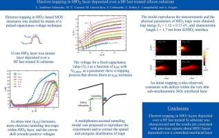
Electron trapping in HfO2-based MOS structures was studied through pulsed capacitance-voltage (C-V) technique. 10 nm HfO2 layer was deposited by atomic layer deposition over a HF last treated Si substrate. The C-V curves were observed to shift to positive voltages driven by the positive applied voltage along the pulses, consistent with electron trapping due to tunneling transitions between the substrate and pre-existing defects within the oxide and the subsequent lattice relaxation through electron-phonon interaction. The dependences of the voltage shift for a given capacitance value (ΔVC) with stress bias and time, allowed to distinguish two mechanisms. An initial trapping process occurs for times shorter than the microsecond, probably associated with a thin non-stoichiometric SiOx interfacial layer, which is followed by a trapping process that starts after tens of μs and progressively slowed down, associated with traps within the HfO2 layer. Numerical simulations yield for the HfO2 traps an energy of 1.3 eV below the conduction band edge, decreasing exponentially with the distance from the Si interface with a characteristic length of 1.7 nm; and phonon and relaxation energies of 50 meV and 1 eV, respectively. These physical parameters are consistent with previous reports of electron trapping in HfO2 layers deposited on a controlled interfacial layer, suggesting that trapping properties of defects inside the HfO2 layer are insensitive to the treatment of the Si surface before HfO2 deposition. On the other hand, the observed large initial trapping suggests that the non-controlled SiOx interfacial region is more defective than a controlled one.
求助全文
通过发布文献求助,成功后即可免费获取论文全文。 去求助
来源期刊
Microelectronic Engineering
Microelectronic Engineering 工程技术-工程:电子与电气
CiteScore
5.30
自引率
4.30%
发文量
131
审稿时长
29 days
期刊介绍: Microelectronic Engineering is the premier nanoprocessing, and nanotechnology journal focusing on fabrication of electronic, photonic, bioelectronic, electromechanic and fluidic devices and systems, and their applications in the broad areas of electronics, photonics, energy, life sciences, and environment. It covers also the expanding interdisciplinary field of "more than Moore" and "beyond Moore" integrated nanoelectronics / photonics and micro-/nano-/bio-systems. Through its unique mixture of peer-reviewed articles, reviews, accelerated publications, short and Technical notes, and the latest research news on key developments, Microelectronic Engineering provides comprehensive coverage of this exciting, interdisciplinary and dynamic new field for researchers in academia and professionals in industry.
×
引用
GB/T 7714-2015
复制
MLA
复制
APA
复制
导出至
BibTeX EndNote RefMan NoteFirst NoteExpress
×
提示
您的信息不完整,为了账户安全,请先补充。
现在去补充
×
提示
您因"违规操作"
具体请查看互助需知
我知道了
×
提示
确定
请完成安全验证×
copy
已复制链接
快去分享给好友吧!
我知道了
右上角分享
点击右上角分享
0
联系我们:info@booksci.cn Book学术提供免费学术资源搜索服务,方便国内外学者检索中英文文献。致力于提供最便捷和优质的服务体验。 Copyright © 2023 布克学术 All rights reserved.
京ICP备2023020795号-1
ghs 京公网安备 11010802042870号
Book学术文献互助
Book学术文献互助群
群 号:481959085
Book学术官方微信