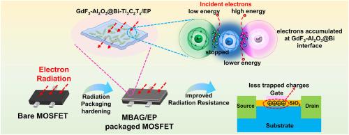
由 Al2O3 诱导的 Bi-GdF3 实现的辐射硬化 MOSFET,Ti3C2Tx 框架中存在被困的界面电子

IF 8.3 1区 材料科学 Q1 MATERIALS SCIENCE, COMPOSITES
Tianyu Zhang , Yang Hong , Jingyang Li , Yang Li , Huiyang Zhao , Kai Cui , Wenjing Wei , Hongjun Kang , Jinzhu Wu , Wei Qin , Xiaohong Wu
{"title":"由 Al2O3 诱导的 Bi-GdF3 实现的辐射硬化 MOSFET,Ti3C2Tx 框架中存在被困的界面电子","authors":"Tianyu Zhang ,&nbsp;Yang Hong ,&nbsp;Jingyang Li ,&nbsp;Yang Li ,&nbsp;Huiyang Zhao ,&nbsp;Kai Cui ,&nbsp;Wenjing Wei ,&nbsp;Hongjun Kang ,&nbsp;Jinzhu Wu ,&nbsp;Wei Qin ,&nbsp;Xiaohong Wu","doi":"10.1016/j.compscitech.2024.110911","DOIUrl":null,"url":null,"abstract":"<div><div>The radiation resistance of Metal-Oxide-Semiconductor Field-Effect Transistors (MOSFETs) is of great significance when applied in aerospace. However, it is still challenging to obtain MOSFETs with excellent radiation resistance. In this work, the radiation hardened MOSFETs were realized by GdF<sub>3</sub>-Al<sub>2</sub>O<sub>3</sub>@Bi-Ti<sub>3</sub>C<sub>2</sub>T<sub><em>x</em></sub>/epoxy (MBAG/EP) polymer-based composite coating with function of trapped interfacial electrons. The radiation resistance of resultant packed MOSFET is significantly improved, showing the lower threshold voltage negative drift value (0.41 V) than the bare MOSFET (7.89 V). This is mainly attributed to the introduction of ultra-thin Al<sub>2</sub>O<sub>3</sub> intermediate layer between Bi and GdF<sub>3</sub>, which effectively tailor electron dense and distribution for an effective electron attenuation, and thus improve the radiation resistance of the MOSFET. Theoretical calculations further reveal that the packed MOSFETs present the less shifted voltage and trapped charges compared with the pristine one. This work provides an interface engineering strategy for developing radiation hardened MOSFETs.</div></div>","PeriodicalId":283,"journal":{"name":"Composites Science and Technology","volume":"258 ","pages":"Article 110911"},"PeriodicalIF":8.3000,"publicationDate":"2024-10-11","publicationTypes":"Journal Article","fieldsOfStudy":null,"isOpenAccess":false,"openAccessPdf":"","citationCount":"0","resultStr":"{\"title\":\"Radiation hardened MOSFETs realized by Al2O3 induced Bi-GdF3 with trapped interfacial electrons located in Ti3C2Tx framework\",\"authors\":\"Tianyu Zhang ,&nbsp;Yang Hong ,&nbsp;Jingyang Li ,&nbsp;Yang Li ,&nbsp;Huiyang Zhao ,&nbsp;Kai Cui ,&nbsp;Wenjing Wei ,&nbsp;Hongjun Kang ,&nbsp;Jinzhu Wu ,&nbsp;Wei Qin ,&nbsp;Xiaohong Wu\",\"doi\":\"10.1016/j.compscitech.2024.110911\",\"DOIUrl\":null,\"url\":null,\"abstract\":\"<div><div>The radiation resistance of Metal-Oxide-Semiconductor Field-Effect Transistors (MOSFETs) is of great significance when applied in aerospace. However, it is still challenging to obtain MOSFETs with excellent radiation resistance. In this work, the radiation hardened MOSFETs were realized by GdF<sub>3</sub>-Al<sub>2</sub>O<sub>3</sub>@Bi-Ti<sub>3</sub>C<sub>2</sub>T<sub><em>x</em></sub>/epoxy (MBAG/EP) polymer-based composite coating with function of trapped interfacial electrons. The radiation resistance of resultant packed MOSFET is significantly improved, showing the lower threshold voltage negative drift value (0.41 V) than the bare MOSFET (7.89 V). This is mainly attributed to the introduction of ultra-thin Al<sub>2</sub>O<sub>3</sub> intermediate layer between Bi and GdF<sub>3</sub>, which effectively tailor electron dense and distribution for an effective electron attenuation, and thus improve the radiation resistance of the MOSFET. Theoretical calculations further reveal that the packed MOSFETs present the less shifted voltage and trapped charges compared with the pristine one. This work provides an interface engineering strategy for developing radiation hardened MOSFETs.</div></div>\",\"PeriodicalId\":283,\"journal\":{\"name\":\"Composites Science and Technology\",\"volume\":\"258 \",\"pages\":\"Article 110911\"},\"PeriodicalIF\":8.3000,\"publicationDate\":\"2024-10-11\",\"publicationTypes\":\"Journal Article\",\"fieldsOfStudy\":null,\"isOpenAccess\":false,\"openAccessPdf\":\"\",\"citationCount\":\"0\",\"resultStr\":null,\"platform\":\"Semanticscholar\",\"paperid\":null,\"PeriodicalName\":\"Composites Science and Technology\",\"FirstCategoryId\":\"88\",\"ListUrlMain\":\"https://www.sciencedirect.com/science/article/pii/S0266353824004810\",\"RegionNum\":1,\"RegionCategory\":\"材料科学\",\"ArticlePicture\":[],\"TitleCN\":null,\"AbstractTextCN\":null,\"PMCID\":null,\"EPubDate\":\"\",\"PubModel\":\"\",\"JCR\":\"Q1\",\"JCRName\":\"MATERIALS SCIENCE, COMPOSITES\",\"Score\":null,\"Total\":0}","platform":"Semanticscholar","paperid":null,"PeriodicalName":"Composites Science and Technology","FirstCategoryId":"88","ListUrlMain":"https://www.sciencedirect.com/science/article/pii/S0266353824004810","RegionNum":1,"RegionCategory":"材料科学","ArticlePicture":[],"TitleCN":null,"AbstractTextCN":null,"PMCID":null,"EPubDate":"","PubModel":"","JCR":"Q1","JCRName":"MATERIALS SCIENCE, COMPOSITES","Score":null,"Total":0}
引用次数: 0

摘要

金属氧化物半导体场效应晶体管(MOSFET)的抗辐射性能在航空航天领域的应用中具有重要意义。然而,要获得具有优异抗辐射性能的 MOSFET 仍然是一项挑战。在这项工作中,通过 GdF3-Al2O3@Bi-Ti3C2Tx/epoxy (MBAG/EP) 聚合物基复合涂层实现了具有捕获界面电子功能的辐射硬化 MOSFET。与裸 MOSFET(7.89 V)相比,封装后的 MOSFET 的抗辐射能力明显提高,阈值电压负漂移值(0.41 V)更低。这主要归功于在 Bi 和 GdF3 之间引入了超薄 Al2O3 中间层,从而有效地调整了电子密度和分布,实现了有效的电子衰减,从而提高了 MOSFET 的辐射阻抗。理论计算进一步表明,与原始 MOSFET 相比,填料 MOSFET 的偏移电压和俘获电荷更少。这项研究为开发抗辐射 MOSFET 提供了一种界面工程策略。
本文章由计算机程序翻译,如有差异,请以英文原文为准。

Radiation hardened MOSFETs realized by Al2O3 induced Bi-GdF3 with trapped interfacial electrons located in Ti3C2Tx framework

Radiation hardened MOSFETs realized by Al2O3 induced Bi-GdF3 with trapped interfacial electrons located in Ti3C2Tx framework
The radiation resistance of Metal-Oxide-Semiconductor Field-Effect Transistors (MOSFETs) is of great significance when applied in aerospace. However, it is still challenging to obtain MOSFETs with excellent radiation resistance. In this work, the radiation hardened MOSFETs were realized by GdF3-Al2O3@Bi-Ti3C2Tx/epoxy (MBAG/EP) polymer-based composite coating with function of trapped interfacial electrons. The radiation resistance of resultant packed MOSFET is significantly improved, showing the lower threshold voltage negative drift value (0.41 V) than the bare MOSFET (7.89 V). This is mainly attributed to the introduction of ultra-thin Al2O3 intermediate layer between Bi and GdF3, which effectively tailor electron dense and distribution for an effective electron attenuation, and thus improve the radiation resistance of the MOSFET. Theoretical calculations further reveal that the packed MOSFETs present the less shifted voltage and trapped charges compared with the pristine one. This work provides an interface engineering strategy for developing radiation hardened MOSFETs.
求助全文
通过发布文献求助,成功后即可免费获取论文全文。 去求助
来源期刊
Composites Science and Technology
Composites Science and Technology 工程技术-材料科学:复合
CiteScore
16.20
自引率
9.90%
发文量
611
审稿时长
33 days
期刊介绍: Composites Science and Technology publishes refereed original articles on the fundamental and applied science of engineering composites. The focus of this journal is on polymeric matrix composites with reinforcements/fillers ranging from nano- to macro-scale. CSTE encourages manuscripts reporting unique, innovative contributions to the physics, chemistry, materials science and applied mechanics aspects of advanced composites. Besides traditional fiber reinforced composites, novel composites with significant potential for engineering applications are encouraged.
×
引用
GB/T 7714-2015
复制
MLA
复制
APA
复制
导出至
BibTeX EndNote RefMan NoteFirst NoteExpress
×
提示
您的信息不完整,为了账户安全,请先补充。
现在去补充
×
提示
您因"违规操作"
具体请查看互助需知
我知道了
×
提示
确定
请完成安全验证×
copy
已复制链接
快去分享给好友吧!
我知道了
右上角分享
点击右上角分享
0
联系我们:info@booksci.cn Book学术提供免费学术资源搜索服务,方便国内外学者检索中英文文献。致力于提供最便捷和优质的服务体验。 Copyright © 2023 布克学术 All rights reserved.
京ICP备2023020795号-1
ghs 京公网安备 11010802042870号
Book学术文献互助
Book学术文献互助群
群 号:481959085
Book学术官方微信