Wangheng Pan, Anran Wang, Xingguang Wu, Xialian Zheng, Hu Chen, Shuchao Qin, Zheng Vitto Han, Siwen Zhao, Rong Zhang and Fengqiu Wang
{"title":"具有超低接触电阻的快速二维 MoS2 光电探测器","authors":"Wangheng Pan, Anran Wang, Xingguang Wu, Xialian Zheng, Hu Chen, Shuchao Qin, Zheng Vitto Han, Siwen Zhao, Rong Zhang and Fengqiu Wang","doi":"10.1039/D4NR02860K","DOIUrl":null,"url":null,"abstract":"<p >Two-dimensional (2D) transition metal dichalcogenides (TMDs), such as molybdenum disulfide (MoS<small><sub>2</sub></small>), hold great promise for next-generation nanoelectronic and nanophotonic devices. While high photoresponsivity and broad spectral coverage (UV–IR) have been reported, the slow response time of MoS<small><sub>2</sub></small> photodetectors caused by their unfavorable RC characteristics is still a major limit in current devices. Once the RC limit issue is resolved, the intrinsic saturation drift velocity of electrons in TMDs (∼10<small><sup>6</sup></small> cm s<small><sup>−1</sup></small>) may enable GHz opto-electronic operations. Recent breakthroughs in device fabrication technology have enabled significant progress in exploring the possibilities of high-speed TMD photodetectors. In this work, using semi-metallic bismuth contacts to suppress metal-induced gap states (MIGS), an MoS<small><sub>2</sub></small> photodetector with ultra-low contact resistance (<400 Ω μm) was fabricated. The device exhibited a broad bandwidth and high photoresponsivity (>1 A W<small><sup>−1</sup></small>). In particular, using an acousto-optic modulator (AOM)-modulated 532 nm laser, a −3 dB cutoff frequency of ∼70 kHz was obtained, which was corroborated by directly observed rise/fall times (on a scale of 10 μs). An extrinsic effect, where defective states of BN induce a negative shift in the photocurrent baseline was further identified and attributed to charge-induced screening, elucidating where a device can exhibit different dynamic and static response behaviors simultaneously. Our results may shed light for future GHz optoelectronic applications employing TMDs as a platform.</p>","PeriodicalId":92,"journal":{"name":"Nanoscale","volume":" 45","pages":" 21061-21067"},"PeriodicalIF":5.1000,"publicationDate":"2024-10-14","publicationTypes":"Journal Article","fieldsOfStudy":null,"isOpenAccess":false,"openAccessPdf":"","citationCount":"0","resultStr":"{\"title\":\"A fast 2D MoS2 photodetector with ultralow contact resistance†\",\"authors\":\"Wangheng Pan, Anran Wang, Xingguang Wu, Xialian Zheng, Hu Chen, Shuchao Qin, Zheng Vitto Han, Siwen Zhao, Rong Zhang and Fengqiu Wang\",\"doi\":\"10.1039/D4NR02860K\",\"DOIUrl\":null,\"url\":null,\"abstract\":\"<p >Two-dimensional (2D) transition metal dichalcogenides (TMDs), such as molybdenum disulfide (MoS<small><sub>2</sub></small>), hold great promise for next-generation nanoelectronic and nanophotonic devices. While high photoresponsivity and broad spectral coverage (UV–IR) have been reported, the slow response time of MoS<small><sub>2</sub></small> photodetectors caused by their unfavorable RC characteristics is still a major limit in current devices. Once the RC limit issue is resolved, the intrinsic saturation drift velocity of electrons in TMDs (∼10<small><sup>6</sup></small> cm s<small><sup>−1</sup></small>) may enable GHz opto-electronic operations. Recent breakthroughs in device fabrication technology have enabled significant progress in exploring the possibilities of high-speed TMD photodetectors. In this work, using semi-metallic bismuth contacts to suppress metal-induced gap states (MIGS), an MoS<small><sub>2</sub></small> photodetector with ultra-low contact resistance (<400 Ω μm) was fabricated. The device exhibited a broad bandwidth and high photoresponsivity (>1 A W<small><sup>−1</sup></small>). In particular, using an acousto-optic modulator (AOM)-modulated 532 nm laser, a −3 dB cutoff frequency of ∼70 kHz was obtained, which was corroborated by directly observed rise/fall times (on a scale of 10 μs). An extrinsic effect, where defective states of BN induce a negative shift in the photocurrent baseline was further identified and attributed to charge-induced screening, elucidating where a device can exhibit different dynamic and static response behaviors simultaneously. Our results may shed light for future GHz optoelectronic applications employing TMDs as a platform.</p>\",\"PeriodicalId\":92,\"journal\":{\"name\":\"Nanoscale\",\"volume\":\" 45\",\"pages\":\" 21061-21067\"},\"PeriodicalIF\":5.1000,\"publicationDate\":\"2024-10-14\",\"publicationTypes\":\"Journal Article\",\"fieldsOfStudy\":null,\"isOpenAccess\":false,\"openAccessPdf\":\"\",\"citationCount\":\"0\",\"resultStr\":null,\"platform\":\"Semanticscholar\",\"paperid\":null,\"PeriodicalName\":\"Nanoscale\",\"FirstCategoryId\":\"88\",\"ListUrlMain\":\"https://pubs.rsc.org/en/content/articlelanding/2024/nr/d4nr02860k\",\"RegionNum\":3,\"RegionCategory\":\"材料科学\",\"ArticlePicture\":[],\"TitleCN\":null,\"AbstractTextCN\":null,\"PMCID\":null,\"EPubDate\":\"\",\"PubModel\":\"\",\"JCR\":\"Q1\",\"JCRName\":\"CHEMISTRY, MULTIDISCIPLINARY\",\"Score\":null,\"Total\":0}","platform":"Semanticscholar","paperid":null,"PeriodicalName":"Nanoscale","FirstCategoryId":"88","ListUrlMain":"https://pubs.rsc.org/en/content/articlelanding/2024/nr/d4nr02860k","RegionNum":3,"RegionCategory":"材料科学","ArticlePicture":[],"TitleCN":null,"AbstractTextCN":null,"PMCID":null,"EPubDate":"","PubModel":"","JCR":"Q1","JCRName":"CHEMISTRY, MULTIDISCIPLINARY","Score":null,"Total":0}
A fast 2D MoS2 photodetector with ultralow contact resistance†
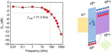
Two-dimensional (2D) transition metal dichalcogenides (TMDs), such as molybdenum disulfide (MoS2), hold great promise for next-generation nanoelectronic and nanophotonic devices. While high photoresponsivity and broad spectral coverage (UV–IR) have been reported, the slow response time of MoS2 photodetectors caused by their unfavorable RC characteristics is still a major limit in current devices. Once the RC limit issue is resolved, the intrinsic saturation drift velocity of electrons in TMDs (∼106 cm s−1) may enable GHz opto-electronic operations. Recent breakthroughs in device fabrication technology have enabled significant progress in exploring the possibilities of high-speed TMD photodetectors. In this work, using semi-metallic bismuth contacts to suppress metal-induced gap states (MIGS), an MoS2 photodetector with ultra-low contact resistance (<400 Ω μm) was fabricated. The device exhibited a broad bandwidth and high photoresponsivity (>1 A W−1). In particular, using an acousto-optic modulator (AOM)-modulated 532 nm laser, a −3 dB cutoff frequency of ∼70 kHz was obtained, which was corroborated by directly observed rise/fall times (on a scale of 10 μs). An extrinsic effect, where defective states of BN induce a negative shift in the photocurrent baseline was further identified and attributed to charge-induced screening, elucidating where a device can exhibit different dynamic and static response behaviors simultaneously. Our results may shed light for future GHz optoelectronic applications employing TMDs as a platform.
期刊介绍:
Nanoscale is a high-impact international journal, publishing high-quality research across nanoscience and nanotechnology. Nanoscale publishes a full mix of research articles on experimental and theoretical work, including reviews, communications, and full papers.Highly interdisciplinary, this journal appeals to scientists, researchers and professionals interested in nanoscience and nanotechnology, quantum materials and quantum technology, including the areas of physics, chemistry, biology, medicine, materials, energy/environment, information technology, detection science, healthcare and drug discovery, and electronics.

 求助内容:
求助内容: 应助结果提醒方式:


