在纸上实现二极管结构:纸上电子学的一个实例

IF 2.4 4区 物理与天体物理 Q3 MATERIALS SCIENCE, MULTIDISCIPLINARY
{"title":"在纸上实现二极管结构:纸上电子学的一个实例","authors":"","doi":"10.1016/j.cap.2024.10.001","DOIUrl":null,"url":null,"abstract":"<div><div>A possibility of fabricating paper/Ag/CdTe/Au Schottky and paper/Ag/CdTe/CdS/In p-n junction diode structures has been demonstrated here. Ag (∼5 μm), CdTe (∼50 μm), CdS (∼45 μm), Au and In dots (∼5 μm) were deposited on the cellulose using appropriate stainless-steel masks to obtain the requisite diode structures. The band gaps of the CdTe and CdS layers were ∼1.55 eV and ∼1.45 eV, respectively. Current-voltage (I-V) characteristics of the paper/Ag/CdTe/Au Schottky and paper/Ag/CdTe/CdS/In p-n junction diodes were recorded at room temperature. Ideality factor (<em>n</em>), series resistance (<em>R</em><sub><em>S</em></sub>) and barrier height (φ<sub>b</sub>) of the respective diodes were computed. The barrier height (φ<sub>b</sub>) and ideality factor (<em>n</em>) computed from current-voltage characteristics were found to be 0.74 eV and 1.8, respectively at room temperature. Series resistance and φ<sub>b</sub> computed by using Cheung-Cheung method were ∼177 Ω and ∼0.45 eV, respectively. They are comparable to the resistance derived from a modified Norde method. The fabricated diodes were reproducible and stable for a few months. These diode structures were tested in an open environment at room temperature and showed no noticeable ageing effect.</div></div>","PeriodicalId":11037,"journal":{"name":"Current Applied Physics","volume":null,"pages":null},"PeriodicalIF":2.4000,"publicationDate":"2024-10-05","publicationTypes":"Journal Article","fieldsOfStudy":null,"isOpenAccess":false,"openAccessPdf":"","citationCount":"0","resultStr":"{\"title\":\"Realization of diode structures on paper: An example of papertronics\",\"authors\":\"\",\"doi\":\"10.1016/j.cap.2024.10.001\",\"DOIUrl\":null,\"url\":null,\"abstract\":\"<div><div>A possibility of fabricating paper/Ag/CdTe/Au Schottky and paper/Ag/CdTe/CdS/In p-n junction diode structures has been demonstrated here. Ag (∼5 μm), CdTe (∼50 μm), CdS (∼45 μm), Au and In dots (∼5 μm) were deposited on the cellulose using appropriate stainless-steel masks to obtain the requisite diode structures. The band gaps of the CdTe and CdS layers were ∼1.55 eV and ∼1.45 eV, respectively. Current-voltage (I-V) characteristics of the paper/Ag/CdTe/Au Schottky and paper/Ag/CdTe/CdS/In p-n junction diodes were recorded at room temperature. Ideality factor (<em>n</em>), series resistance (<em>R</em><sub><em>S</em></sub>) and barrier height (φ<sub>b</sub>) of the respective diodes were computed. The barrier height (φ<sub>b</sub>) and ideality factor (<em>n</em>) computed from current-voltage characteristics were found to be 0.74 eV and 1.8, respectively at room temperature. Series resistance and φ<sub>b</sub> computed by using Cheung-Cheung method were ∼177 Ω and ∼0.45 eV, respectively. They are comparable to the resistance derived from a modified Norde method. The fabricated diodes were reproducible and stable for a few months. These diode structures were tested in an open environment at room temperature and showed no noticeable ageing effect.</div></div>\",\"PeriodicalId\":11037,\"journal\":{\"name\":\"Current Applied Physics\",\"volume\":null,\"pages\":null},\"PeriodicalIF\":2.4000,\"publicationDate\":\"2024-10-05\",\"publicationTypes\":\"Journal Article\",\"fieldsOfStudy\":null,\"isOpenAccess\":false,\"openAccessPdf\":\"\",\"citationCount\":\"0\",\"resultStr\":null,\"platform\":\"Semanticscholar\",\"paperid\":null,\"PeriodicalName\":\"Current Applied Physics\",\"FirstCategoryId\":\"101\",\"ListUrlMain\":\"https://www.sciencedirect.com/science/article/pii/S1567173924002141\",\"RegionNum\":4,\"RegionCategory\":\"物理与天体物理\",\"ArticlePicture\":[],\"TitleCN\":null,\"AbstractTextCN\":null,\"PMCID\":null,\"EPubDate\":\"\",\"PubModel\":\"\",\"JCR\":\"Q3\",\"JCRName\":\"MATERIALS SCIENCE, MULTIDISCIPLINARY\",\"Score\":null,\"Total\":0}","platform":"Semanticscholar","paperid":null,"PeriodicalName":"Current Applied Physics","FirstCategoryId":"101","ListUrlMain":"https://www.sciencedirect.com/science/article/pii/S1567173924002141","RegionNum":4,"RegionCategory":"物理与天体物理","ArticlePicture":[],"TitleCN":null,"AbstractTextCN":null,"PMCID":null,"EPubDate":"","PubModel":"","JCR":"Q3","JCRName":"MATERIALS SCIENCE, MULTIDISCIPLINARY","Score":null,"Total":0}
引用次数: 0

摘要

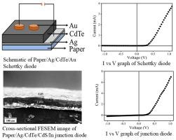
本文展示了制造纸/银/碲化镉/金肖特基二极管和纸/银/碲化镉/镉硒/铟 p-n 结二极管结构的可能性。使用适当的不锈钢掩膜在纤维素上沉积银(5 μm)、碲化镉(50 μm)、硒化镉(45 μm)、金和铟点(5 μm),以获得所需的二极管结构。碲化镉层和硒化镉层的带隙分别为 1.55 eV 和 1.45 eV。室温下记录了纸/银/CdTe/金肖特基二极管和纸/银/CdTe/CdS/铟 p-n 结二极管的电流-电压(I-V)特性。计算了各二极管的理想因子 (n)、串联电阻 (RS) 和势垒高度 (φb)。根据电流-电压特性计算得出的势垒高度(φb)和理想化系数(n)在室温下分别为 0.74 eV 和 1.8。用 Cheung-Cheung 方法计算出的串联电阻和φb 分别为 177 Ω 和 0.45 eV。这两个数值与改进 Norde 方法得出的电阻值相当。制作的二极管在几个月内都是可重复和稳定的。这些二极管结构在室温下的开放环境中进行了测试,没有显示出明显的老化效应。
本文章由计算机程序翻译,如有差异,请以英文原文为准。

Realization of diode structures on paper: An example of papertronics

Realization of diode structures on paper: An example of papertronics
A possibility of fabricating paper/Ag/CdTe/Au Schottky and paper/Ag/CdTe/CdS/In p-n junction diode structures has been demonstrated here. Ag (∼5 μm), CdTe (∼50 μm), CdS (∼45 μm), Au and In dots (∼5 μm) were deposited on the cellulose using appropriate stainless-steel masks to obtain the requisite diode structures. The band gaps of the CdTe and CdS layers were ∼1.55 eV and ∼1.45 eV, respectively. Current-voltage (I-V) characteristics of the paper/Ag/CdTe/Au Schottky and paper/Ag/CdTe/CdS/In p-n junction diodes were recorded at room temperature. Ideality factor (n), series resistance (RS) and barrier height (φb) of the respective diodes were computed. The barrier height (φb) and ideality factor (n) computed from current-voltage characteristics were found to be 0.74 eV and 1.8, respectively at room temperature. Series resistance and φb computed by using Cheung-Cheung method were ∼177 Ω and ∼0.45 eV, respectively. They are comparable to the resistance derived from a modified Norde method. The fabricated diodes were reproducible and stable for a few months. These diode structures were tested in an open environment at room temperature and showed no noticeable ageing effect.
求助全文
通过发布文献求助,成功后即可免费获取论文全文。 去求助
来源期刊
Current Applied Physics
Current Applied Physics 物理-材料科学:综合
CiteScore
4.80
自引率
0.00%
发文量
213
审稿时长
33 days
期刊介绍: Current Applied Physics (Curr. Appl. Phys.) is a monthly published international journal covering all the fields of applied science investigating the physics of the advanced materials for future applications. Other areas covered: Experimental and theoretical aspects of advanced materials and devices dealing with synthesis or structural chemistry, physical and electronic properties, photonics, engineering applications, and uniquely pertinent measurement or analytical techniques. Current Applied Physics, published since 2001, covers physics, chemistry and materials science, including bio-materials, with their engineering aspects. It is a truly interdisciplinary journal opening a forum for scientists of all related fields, a unique point of the journal discriminating it from other worldwide and/or Pacific Rim applied physics journals. Regular research papers, letters and review articles with contents meeting the scope of the journal will be considered for publication after peer review. The Journal is owned by the Korean Physical Society.
×
引用
GB/T 7714-2015
复制
MLA
复制
APA
复制
导出至
BibTeX EndNote RefMan NoteFirst NoteExpress
×
提示
您的信息不完整,为了账户安全,请先补充。
现在去补充
×
提示
您因"违规操作"
具体请查看互助需知
我知道了
×
提示
确定
请完成安全验证×
copy
已复制链接
快去分享给好友吧!
我知道了
右上角分享
点击右上角分享
0
联系我们:info@booksci.cn Book学术提供免费学术资源搜索服务,方便国内外学者检索中英文文献。致力于提供最便捷和优质的服务体验。 Copyright © 2023 布克学术 All rights reserved.
京ICP备2023020795号-1
ghs 京公网安备 11010802042870号
Book学术文献互助
Book学术文献互助群
群 号:481959085
Book学术官方微信