在微球光刻法刻画的硅晶片上选择性区域外延磷化镓基纳米结构,用于可见光光电技术

IF 5.3 3区 材料科学 Q2 MATERIALS SCIENCE, MULTIDISCIPLINARY
Liliia N. Dvoretckaia , Vladimir V. Fedorov , Alexander Pavlov , Sergey D. Komarov , Eduard I. Moiseev , Dmitry V. Miniv , Andrey K. Kaveev , Aliaksandr G. Smirnov , Demid A. Kirilenko , Alexey M. Mozharov , Ivan S. Mukhin
{"title":"在微球光刻法刻画的硅晶片上选择性区域外延磷化镓基纳米结构,用于可见光光电技术","authors":"Liliia N. Dvoretckaia ,&nbsp;Vladimir V. Fedorov ,&nbsp;Alexander Pavlov ,&nbsp;Sergey D. Komarov ,&nbsp;Eduard I. Moiseev ,&nbsp;Dmitry V. Miniv ,&nbsp;Andrey K. Kaveev ,&nbsp;Aliaksandr G. Smirnov ,&nbsp;Demid A. Kirilenko ,&nbsp;Alexey M. Mozharov ,&nbsp;Ivan S. Mukhin","doi":"10.1016/j.materresbull.2024.113126","DOIUrl":null,"url":null,"abstract":"<div><div>In this study, we present the selective area plasma-assisted molecular beam epitaxial growth of GaP-based nanoheterostructures (nanostubs), incorporating direct bandgap GaAsP or GaPN segments, on patterned SiO<sub>2</sub>/Si(001) wafers. A microsphere optical lithography and anisotropic Si wet-etching techniques were employed for wafer-scale surface patterning through SiO<sub>2</sub> growth mask, allowing to obtain either planar or pyramidal pit nucleation site morphologies. X-ray diffraction reciprocal space mapping and Raman microspectroscopy studies confirm compositional homogeneity of the nanostub arrays. The dilute nitride nanostubs display the narrowest and most intense visible red photoluminescence response at room temperature, which is an order of magnitude higher compared to the GaAsP ones. The formation of the nitrogen sub-band in GaPN alloy was confirmed in the framework of density functional theory, providing insights for interpreting the experimental results. These findings demonstrate the feasibility of the proposed approach for fabricating the ordered arrays of nanoscale visible light emitters on silicon.</div></div>","PeriodicalId":18265,"journal":{"name":"Materials Research Bulletin","volume":"182 ","pages":"Article 113126"},"PeriodicalIF":5.3000,"publicationDate":"2024-10-05","publicationTypes":"Journal Article","fieldsOfStudy":null,"isOpenAccess":false,"openAccessPdf":"","citationCount":"0","resultStr":"{\"title\":\"Selective area epitaxy of gallium phosphide-based nanostructures on microsphere lithography-patterned Si wafers for visible light optoelectronics\",\"authors\":\"Liliia N. Dvoretckaia ,&nbsp;Vladimir V. Fedorov ,&nbsp;Alexander Pavlov ,&nbsp;Sergey D. Komarov ,&nbsp;Eduard I. Moiseev ,&nbsp;Dmitry V. Miniv ,&nbsp;Andrey K. Kaveev ,&nbsp;Aliaksandr G. Smirnov ,&nbsp;Demid A. Kirilenko ,&nbsp;Alexey M. Mozharov ,&nbsp;Ivan S. Mukhin\",\"doi\":\"10.1016/j.materresbull.2024.113126\",\"DOIUrl\":null,\"url\":null,\"abstract\":\"<div><div>In this study, we present the selective area plasma-assisted molecular beam epitaxial growth of GaP-based nanoheterostructures (nanostubs), incorporating direct bandgap GaAsP or GaPN segments, on patterned SiO<sub>2</sub>/Si(001) wafers. A microsphere optical lithography and anisotropic Si wet-etching techniques were employed for wafer-scale surface patterning through SiO<sub>2</sub> growth mask, allowing to obtain either planar or pyramidal pit nucleation site morphologies. X-ray diffraction reciprocal space mapping and Raman microspectroscopy studies confirm compositional homogeneity of the nanostub arrays. The dilute nitride nanostubs display the narrowest and most intense visible red photoluminescence response at room temperature, which is an order of magnitude higher compared to the GaAsP ones. The formation of the nitrogen sub-band in GaPN alloy was confirmed in the framework of density functional theory, providing insights for interpreting the experimental results. These findings demonstrate the feasibility of the proposed approach for fabricating the ordered arrays of nanoscale visible light emitters on silicon.</div></div>\",\"PeriodicalId\":18265,\"journal\":{\"name\":\"Materials Research Bulletin\",\"volume\":\"182 \",\"pages\":\"Article 113126\"},\"PeriodicalIF\":5.3000,\"publicationDate\":\"2024-10-05\",\"publicationTypes\":\"Journal Article\",\"fieldsOfStudy\":null,\"isOpenAccess\":false,\"openAccessPdf\":\"\",\"citationCount\":\"0\",\"resultStr\":null,\"platform\":\"Semanticscholar\",\"paperid\":null,\"PeriodicalName\":\"Materials Research Bulletin\",\"FirstCategoryId\":\"88\",\"ListUrlMain\":\"https://www.sciencedirect.com/science/article/pii/S0025540824004562\",\"RegionNum\":3,\"RegionCategory\":\"材料科学\",\"ArticlePicture\":[],\"TitleCN\":null,\"AbstractTextCN\":null,\"PMCID\":null,\"EPubDate\":\"\",\"PubModel\":\"\",\"JCR\":\"Q2\",\"JCRName\":\"MATERIALS SCIENCE, MULTIDISCIPLINARY\",\"Score\":null,\"Total\":0}","platform":"Semanticscholar","paperid":null,"PeriodicalName":"Materials Research Bulletin","FirstCategoryId":"88","ListUrlMain":"https://www.sciencedirect.com/science/article/pii/S0025540824004562","RegionNum":3,"RegionCategory":"材料科学","ArticlePicture":[],"TitleCN":null,"AbstractTextCN":null,"PMCID":null,"EPubDate":"","PubModel":"","JCR":"Q2","JCRName":"MATERIALS SCIENCE, MULTIDISCIPLINARY","Score":null,"Total":0}
引用次数: 0

摘要

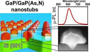
在这项研究中,我们介绍了选择性区域等离子体辅助分子束外延生长基于 GaP 的纳米异质结构(纳米管)的方法,这种纳米异质结构在图案化的二氧化硅/硅(001)晶片上结合了直接带隙 GaAsP 或 GaPN 段。采用微球光学光刻和各向异性硅湿蚀刻技术,通过二氧化硅生长掩模进行晶圆级表面图案化,从而获得平面或金字塔凹坑成核点形态。X 射线衍射倒易空间图谱和拉曼微光谱研究证实了纳米管阵列的成分均匀性。稀氮化物纳米管在室温下显示出最窄、最强烈的可见红色光致发光响应,比砷化镓纳米管高出一个数量级。密度泛函理论框架证实了氮化镓合金中氮子带的形成,为解释实验结果提供了启示。这些发现证明了在硅上制造有序的纳米级可见光发射器阵列的可行性。
本文章由计算机程序翻译,如有差异,请以英文原文为准。

Selective area epitaxy of gallium phosphide-based nanostructures on microsphere lithography-patterned Si wafers for visible light optoelectronics

Selective area epitaxy of gallium phosphide-based nanostructures on microsphere lithography-patterned Si wafers for visible light optoelectronics
In this study, we present the selective area plasma-assisted molecular beam epitaxial growth of GaP-based nanoheterostructures (nanostubs), incorporating direct bandgap GaAsP or GaPN segments, on patterned SiO2/Si(001) wafers. A microsphere optical lithography and anisotropic Si wet-etching techniques were employed for wafer-scale surface patterning through SiO2 growth mask, allowing to obtain either planar or pyramidal pit nucleation site morphologies. X-ray diffraction reciprocal space mapping and Raman microspectroscopy studies confirm compositional homogeneity of the nanostub arrays. The dilute nitride nanostubs display the narrowest and most intense visible red photoluminescence response at room temperature, which is an order of magnitude higher compared to the GaAsP ones. The formation of the nitrogen sub-band in GaPN alloy was confirmed in the framework of density functional theory, providing insights for interpreting the experimental results. These findings demonstrate the feasibility of the proposed approach for fabricating the ordered arrays of nanoscale visible light emitters on silicon.
求助全文
通过发布文献求助,成功后即可免费获取论文全文。 去求助
来源期刊
Materials Research Bulletin
Materials Research Bulletin 工程技术-材料科学:综合
CiteScore
9.80
自引率
5.60%
发文量
372
审稿时长
42 days
期刊介绍: Materials Research Bulletin is an international journal reporting high-impact research on processing-structure-property relationships in functional materials and nanomaterials with interesting electronic, magnetic, optical, thermal, mechanical or catalytic properties. Papers purely on thermodynamics or theoretical calculations (e.g., density functional theory) do not fall within the scope of the journal unless they also demonstrate a clear link to physical properties. Topics covered include functional materials (e.g., dielectrics, pyroelectrics, piezoelectrics, ferroelectrics, relaxors, thermoelectrics, etc.); electrochemistry and solid-state ionics (e.g., photovoltaics, batteries, sensors, and fuel cells); nanomaterials, graphene, and nanocomposites; luminescence and photocatalysis; crystal-structure and defect-structure analysis; novel electronics; non-crystalline solids; flexible electronics; protein-material interactions; and polymeric ion-exchange membranes.
×
引用
GB/T 7714-2015
复制
MLA
复制
APA
复制
导出至
BibTeX EndNote RefMan NoteFirst NoteExpress
×
提示
您的信息不完整,为了账户安全,请先补充。
现在去补充
×
提示
您因"违规操作"
具体请查看互助需知
我知道了
×
提示
确定
请完成安全验证×
copy
已复制链接
快去分享给好友吧!
我知道了
右上角分享
点击右上角分享
0
联系我们:info@booksci.cn Book学术提供免费学术资源搜索服务,方便国内外学者检索中英文文献。致力于提供最便捷和优质的服务体验。 Copyright © 2023 布克学术 All rights reserved.
京ICP备2023020795号-1
ghs 京公网安备 11010802042870号
Book学术文献互助
Book学术文献互助群
群 号:481959085
Book学术官方微信