Gyu-Won Han, Jaewon Jang, Minsu Park, Hui Jae Cho, Jungchul Song, Yeonsang Park
{"title":"在 CMOS 平台上大规模制造具有圆极化功能的元轴晶","authors":"Gyu-Won Han, Jaewon Jang, Minsu Park, Hui Jae Cho, Jungchul Song, Yeonsang Park","doi":"10.1515/nanoph-2024-0413","DOIUrl":null,"url":null,"abstract":"Metasurfaces, consisting of arrays of subwavelength structures, are lightweight and compact while being capable of implementing the functions of traditional bulky optical components. Furthermore, they have the potential to significantly improve complex optical systems in terms of space and cost, as they can simultaneously implement multiple functions. The wafer-scale mass production method based on the CMOS (complementary metal oxide semiconductor) process plays a crucial role in the modern semiconductor industry. This approach can also be applied to the production of metasurfaces, thereby accelerating the entry of metasurfaces into industrial applications. In this study, we demonstrated the mass production of large-area <jats:italic>meta</jats:italic>-axicons with a diameter of 2 mm on an 8-inch wafer using DUV (Deep Ultraviolet) photolithography. The proposed <jats:italic>meta</jats:italic>-axicon designed here is based on PB (Pancharatnam–Berry) phase and is engineered to simultaneously modulate the phase and polarization of light. In practice, the fabricated <jats:italic>meta</jats:italic>-axicon generated a circularly polarized Bessel beam with a depth of focus (DoF) of approximately 2.3 mm in the vicinity of 980 nm. We anticipate that the mass production of large-area <jats:italic>meta</jats:italic>-axicons on this CMOS platform can offer various advantages in optical communication, laser drilling, optical trapping, and tweezing applications.","PeriodicalId":19027,"journal":{"name":"Nanophotonics","volume":"7 1","pages":""},"PeriodicalIF":6.5000,"publicationDate":"2024-10-08","publicationTypes":"Journal Article","fieldsOfStudy":null,"isOpenAccess":false,"openAccessPdf":"","citationCount":"0","resultStr":"{\"title\":\"Large-scale fabrication of meta-axicon with circular polarization on CMOS platform\",\"authors\":\"Gyu-Won Han, Jaewon Jang, Minsu Park, Hui Jae Cho, Jungchul Song, Yeonsang Park\",\"doi\":\"10.1515/nanoph-2024-0413\",\"DOIUrl\":null,\"url\":null,\"abstract\":\"Metasurfaces, consisting of arrays of subwavelength structures, are lightweight and compact while being capable of implementing the functions of traditional bulky optical components. Furthermore, they have the potential to significantly improve complex optical systems in terms of space and cost, as they can simultaneously implement multiple functions. The wafer-scale mass production method based on the CMOS (complementary metal oxide semiconductor) process plays a crucial role in the modern semiconductor industry. This approach can also be applied to the production of metasurfaces, thereby accelerating the entry of metasurfaces into industrial applications. In this study, we demonstrated the mass production of large-area <jats:italic>meta</jats:italic>-axicons with a diameter of 2 mm on an 8-inch wafer using DUV (Deep Ultraviolet) photolithography. The proposed <jats:italic>meta</jats:italic>-axicon designed here is based on PB (Pancharatnam–Berry) phase and is engineered to simultaneously modulate the phase and polarization of light. In practice, the fabricated <jats:italic>meta</jats:italic>-axicon generated a circularly polarized Bessel beam with a depth of focus (DoF) of approximately 2.3 mm in the vicinity of 980 nm. We anticipate that the mass production of large-area <jats:italic>meta</jats:italic>-axicons on this CMOS platform can offer various advantages in optical communication, laser drilling, optical trapping, and tweezing applications.\",\"PeriodicalId\":19027,\"journal\":{\"name\":\"Nanophotonics\",\"volume\":\"7 1\",\"pages\":\"\"},\"PeriodicalIF\":6.5000,\"publicationDate\":\"2024-10-08\",\"publicationTypes\":\"Journal Article\",\"fieldsOfStudy\":null,\"isOpenAccess\":false,\"openAccessPdf\":\"\",\"citationCount\":\"0\",\"resultStr\":null,\"platform\":\"Semanticscholar\",\"paperid\":null,\"PeriodicalName\":\"Nanophotonics\",\"FirstCategoryId\":\"101\",\"ListUrlMain\":\"https://doi.org/10.1515/nanoph-2024-0413\",\"RegionNum\":2,\"RegionCategory\":\"物理与天体物理\",\"ArticlePicture\":[],\"TitleCN\":null,\"AbstractTextCN\":null,\"PMCID\":null,\"EPubDate\":\"\",\"PubModel\":\"\",\"JCR\":\"Q1\",\"JCRName\":\"MATERIALS SCIENCE, MULTIDISCIPLINARY\",\"Score\":null,\"Total\":0}","platform":"Semanticscholar","paperid":null,"PeriodicalName":"Nanophotonics","FirstCategoryId":"101","ListUrlMain":"https://doi.org/10.1515/nanoph-2024-0413","RegionNum":2,"RegionCategory":"物理与天体物理","ArticlePicture":[],"TitleCN":null,"AbstractTextCN":null,"PMCID":null,"EPubDate":"","PubModel":"","JCR":"Q1","JCRName":"MATERIALS SCIENCE, MULTIDISCIPLINARY","Score":null,"Total":0}
Large-scale fabrication of meta-axicon with circular polarization on CMOS platform
Metasurfaces, consisting of arrays of subwavelength structures, are lightweight and compact while being capable of implementing the functions of traditional bulky optical components. Furthermore, they have the potential to significantly improve complex optical systems in terms of space and cost, as they can simultaneously implement multiple functions. The wafer-scale mass production method based on the CMOS (complementary metal oxide semiconductor) process plays a crucial role in the modern semiconductor industry. This approach can also be applied to the production of metasurfaces, thereby accelerating the entry of metasurfaces into industrial applications. In this study, we demonstrated the mass production of large-area meta-axicons with a diameter of 2 mm on an 8-inch wafer using DUV (Deep Ultraviolet) photolithography. The proposed meta-axicon designed here is based on PB (Pancharatnam–Berry) phase and is engineered to simultaneously modulate the phase and polarization of light. In practice, the fabricated meta-axicon generated a circularly polarized Bessel beam with a depth of focus (DoF) of approximately 2.3 mm in the vicinity of 980 nm. We anticipate that the mass production of large-area meta-axicons on this CMOS platform can offer various advantages in optical communication, laser drilling, optical trapping, and tweezing applications.
期刊介绍:
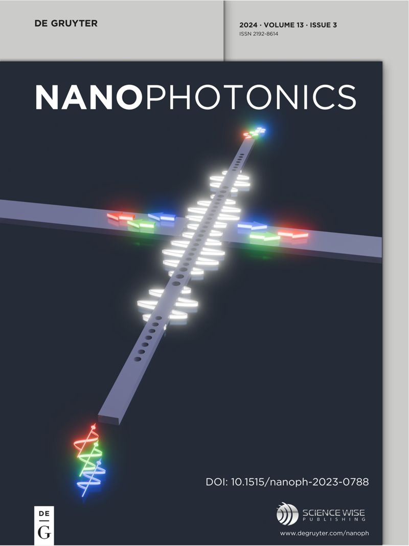
Nanophotonics, published in collaboration with Sciencewise, is a prestigious journal that showcases recent international research results, notable advancements in the field, and innovative applications. It is regarded as one of the leading publications in the realm of nanophotonics and encompasses a range of article types including research articles, selectively invited reviews, letters, and perspectives.
The journal specifically delves into the study of photon interaction with nano-structures, such as carbon nano-tubes, nano metal particles, nano crystals, semiconductor nano dots, photonic crystals, tissue, and DNA. It offers comprehensive coverage of the most up-to-date discoveries, making it an essential resource for physicists, engineers, and material scientists.