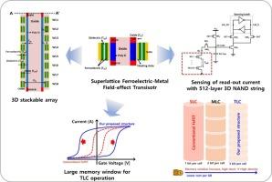
为三级单元 3D NAND 闪存设计超晶格铁电-金属场效应晶体管

IF 2.6 4区 工程技术 Q2 ENGINEERING, ELECTRICAL & ELECTRONIC
Sola Woo , Gihun Choe , Asif Islam Khan , Suman Datta , Shimeng Yu
{"title":"为三级单元 3D NAND 闪存设计超晶格铁电-金属场效应晶体管","authors":"Sola Woo ,&nbsp;Gihun Choe ,&nbsp;Asif Islam Khan ,&nbsp;Suman Datta ,&nbsp;Shimeng Yu","doi":"10.1016/j.mee.2024.112276","DOIUrl":null,"url":null,"abstract":"<div><div>Superlattice ferroelectric-metal field-effect transistor (SL-FeMFET) based three-dimensional NAND architecture (3D NAND) is investigated for triple-level cell (TLC) operations. The SL-FeMFET shows a novel approach for designing the gate-stack using a superlattice of ferroelectric/dielectric/ferroelectric for achieving large memory window ∼3.48 V with program/erase voltage ±7 V for 3D NAND architecture. By TCAD modeling, we demonstrate TLC operation of SL-FeMFET with improving memory window and alleviating variability caused by floating metal layer in FeMFET structure. In addition, as the vertical gate stack increases from 256-layer to 512-layer, the read-out current with worst cases in seven read operations for TLC sensing are examined using page buffer circuit for sensing operation. The simulation results suggest that SL-FeMFET based 3D NAND architecture can operate 512-layer with sufficient sense margin for TLC operation.</div></div>","PeriodicalId":18557,"journal":{"name":"Microelectronic Engineering","volume":"295 ","pages":"Article 112276"},"PeriodicalIF":2.6000,"publicationDate":"2024-09-24","publicationTypes":"Journal Article","fieldsOfStudy":null,"isOpenAccess":false,"openAccessPdf":"","citationCount":"0","resultStr":"{\"title\":\"Design of Superlattice Ferroelectric-Metal Field-effect Transistor for triple-level cell 3D NAND flash\",\"authors\":\"Sola Woo ,&nbsp;Gihun Choe ,&nbsp;Asif Islam Khan ,&nbsp;Suman Datta ,&nbsp;Shimeng Yu\",\"doi\":\"10.1016/j.mee.2024.112276\",\"DOIUrl\":null,\"url\":null,\"abstract\":\"<div><div>Superlattice ferroelectric-metal field-effect transistor (SL-FeMFET) based three-dimensional NAND architecture (3D NAND) is investigated for triple-level cell (TLC) operations. The SL-FeMFET shows a novel approach for designing the gate-stack using a superlattice of ferroelectric/dielectric/ferroelectric for achieving large memory window ∼3.48 V with program/erase voltage ±7 V for 3D NAND architecture. By TCAD modeling, we demonstrate TLC operation of SL-FeMFET with improving memory window and alleviating variability caused by floating metal layer in FeMFET structure. In addition, as the vertical gate stack increases from 256-layer to 512-layer, the read-out current with worst cases in seven read operations for TLC sensing are examined using page buffer circuit for sensing operation. The simulation results suggest that SL-FeMFET based 3D NAND architecture can operate 512-layer with sufficient sense margin for TLC operation.</div></div>\",\"PeriodicalId\":18557,\"journal\":{\"name\":\"Microelectronic Engineering\",\"volume\":\"295 \",\"pages\":\"Article 112276\"},\"PeriodicalIF\":2.6000,\"publicationDate\":\"2024-09-24\",\"publicationTypes\":\"Journal Article\",\"fieldsOfStudy\":null,\"isOpenAccess\":false,\"openAccessPdf\":\"\",\"citationCount\":\"0\",\"resultStr\":null,\"platform\":\"Semanticscholar\",\"paperid\":null,\"PeriodicalName\":\"Microelectronic Engineering\",\"FirstCategoryId\":\"5\",\"ListUrlMain\":\"https://www.sciencedirect.com/science/article/pii/S016793172400145X\",\"RegionNum\":4,\"RegionCategory\":\"工程技术\",\"ArticlePicture\":[],\"TitleCN\":null,\"AbstractTextCN\":null,\"PMCID\":null,\"EPubDate\":\"\",\"PubModel\":\"\",\"JCR\":\"Q2\",\"JCRName\":\"ENGINEERING, ELECTRICAL & ELECTRONIC\",\"Score\":null,\"Total\":0}","platform":"Semanticscholar","paperid":null,"PeriodicalName":"Microelectronic Engineering","FirstCategoryId":"5","ListUrlMain":"https://www.sciencedirect.com/science/article/pii/S016793172400145X","RegionNum":4,"RegionCategory":"工程技术","ArticlePicture":[],"TitleCN":null,"AbstractTextCN":null,"PMCID":null,"EPubDate":"","PubModel":"","JCR":"Q2","JCRName":"ENGINEERING, ELECTRICAL & ELECTRONIC","Score":null,"Total":0}
引用次数: 0

摘要

研究了基于超晶格铁电-金属场效应晶体管(SL-FeMFET)的三维 NAND 架构(3D NAND),用于三电平单元(TLC)操作。SL-FeMFET 展示了一种使用铁电/介电/铁电超晶格设计栅极堆栈的新方法,可实现 3D NAND 架构的大内存窗口 ∼ 3.48 V,程序/擦除电压为 ±7 V。通过 TCAD 建模,我们演示了 SL-FeMFET 的 TLC 运行,改善了存储器窗口,并减轻了 FeMFET 结构中浮动金属层引起的变化。此外,当垂直栅极堆叠从 256 层增加到 512 层时,我们使用页面缓冲电路对 TLC 检测的读出电流和 7 次读取操作中的最坏情况进行了研究。仿真结果表明,基于 SL-FeMFET 的 3D NAND 架构可以在 512 层上运行,并为 TLC 运行提供足够的感应裕量。
本文章由计算机程序翻译,如有差异,请以英文原文为准。

Design of Superlattice Ferroelectric-Metal Field-effect Transistor for triple-level cell 3D NAND flash

Design of Superlattice Ferroelectric-Metal Field-effect Transistor for triple-level cell 3D NAND flash
Superlattice ferroelectric-metal field-effect transistor (SL-FeMFET) based three-dimensional NAND architecture (3D NAND) is investigated for triple-level cell (TLC) operations. The SL-FeMFET shows a novel approach for designing the gate-stack using a superlattice of ferroelectric/dielectric/ferroelectric for achieving large memory window ∼3.48 V with program/erase voltage ±7 V for 3D NAND architecture. By TCAD modeling, we demonstrate TLC operation of SL-FeMFET with improving memory window and alleviating variability caused by floating metal layer in FeMFET structure. In addition, as the vertical gate stack increases from 256-layer to 512-layer, the read-out current with worst cases in seven read operations for TLC sensing are examined using page buffer circuit for sensing operation. The simulation results suggest that SL-FeMFET based 3D NAND architecture can operate 512-layer with sufficient sense margin for TLC operation.
求助全文
通过发布文献求助,成功后即可免费获取论文全文。 去求助
来源期刊
Microelectronic Engineering
Microelectronic Engineering 工程技术-工程:电子与电气
CiteScore
5.30
自引率
4.30%
发文量
131
审稿时长
29 days
期刊介绍: Microelectronic Engineering is the premier nanoprocessing, and nanotechnology journal focusing on fabrication of electronic, photonic, bioelectronic, electromechanic and fluidic devices and systems, and their applications in the broad areas of electronics, photonics, energy, life sciences, and environment. It covers also the expanding interdisciplinary field of "more than Moore" and "beyond Moore" integrated nanoelectronics / photonics and micro-/nano-/bio-systems. Through its unique mixture of peer-reviewed articles, reviews, accelerated publications, short and Technical notes, and the latest research news on key developments, Microelectronic Engineering provides comprehensive coverage of this exciting, interdisciplinary and dynamic new field for researchers in academia and professionals in industry.
×
引用
GB/T 7714-2015
复制
MLA
复制
APA
复制
导出至
BibTeX EndNote RefMan NoteFirst NoteExpress
×
提示
您的信息不完整,为了账户安全,请先补充。
现在去补充
×
提示
您因"违规操作"
具体请查看互助需知
我知道了
×
提示
确定
请完成安全验证×
copy
已复制链接
快去分享给好友吧!
我知道了
右上角分享
点击右上角分享
0
联系我们:info@booksci.cn Book学术提供免费学术资源搜索服务,方便国内外学者检索中英文文献。致力于提供最便捷和优质的服务体验。 Copyright © 2023 布克学术 All rights reserved.
京ICP备2023020795号-1
ghs 京公网安备 11010802042870号
Book学术文献互助
Book学术文献互助群
群 号:481959085
Book学术官方微信