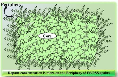
利用先进的调频静电力显微镜对 PANI/PSS 薄膜中的电荷/掺杂剂分布进行直接成像

IF 4.3 3区 材料科学 Q1 ENGINEERING, ELECTRICAL & ELECTRONIC
Priyanka Ranka, Virendra Sethi, Aliasgar Q. Contractor
{"title":"利用先进的调频静电力显微镜对 PANI/PSS 薄膜中的电荷/掺杂剂分布进行直接成像","authors":"Priyanka Ranka, Virendra Sethi, Aliasgar Q. Contractor","doi":"10.1021/acs.langmuir.4c02012","DOIUrl":null,"url":null,"abstract":"This paper presents a detailed study that maps the surface charges and dopant distribution on the electropolymerized thin film of polyaniline–poly(styrenesulfonate) (PANI/PSS). The focus is on two distinct states of PANI/PSS: the fully doped emeraldine salt (ES/PSS) and the dedoped emeraldine base (EB/PSS). This investigation utilizes advanced frequency modulation electrostatic force microscopy (FM-EFM) and atomic force microscopy (AFM). The polymer film comprises polymer grains, and FM-EFM data suggest a non-uniform distribution of dopants on the grain surface, with a higher doped periphery than the core. Quantifying the charge at the periphery and core of ES/PSS and EB/PSS grains provides unique insight into the charge distribution within the polymer film. The charge density is estimated to be 10 times higher in the periphery region (∼120 μC/cm<sup>2</sup>) than in the core region (∼11 μC/cm<sup>2</sup>) and 100 times higher than EB/PSS (∼0.8 μC/cm<sup>2</sup>). We have directly observed the morphological changes of PANI/PSS from the ES/PSS state to the EB/PSS state using the AFM topographic profile. These findings provide a better understanding of the behavior of the charge/dopant distribution on the surface of the polymer films and pave the way for further research and development of PANI/PSS-based electronic devices.","PeriodicalId":3,"journal":{"name":"ACS Applied Electronic Materials","volume":null,"pages":null},"PeriodicalIF":4.3000,"publicationDate":"2024-09-24","publicationTypes":"Journal Article","fieldsOfStudy":null,"isOpenAccess":false,"openAccessPdf":"","citationCount":"0","resultStr":"{\"title\":\"Direct Imaging of Charge/Dopant Distribution in PANI/PSS Thin Films Using Advanced Frequency Modulation Electrostatic Force Microscopy\",\"authors\":\"Priyanka Ranka, Virendra Sethi, Aliasgar Q. Contractor\",\"doi\":\"10.1021/acs.langmuir.4c02012\",\"DOIUrl\":null,\"url\":null,\"abstract\":\"This paper presents a detailed study that maps the surface charges and dopant distribution on the electropolymerized thin film of polyaniline–poly(styrenesulfonate) (PANI/PSS). The focus is on two distinct states of PANI/PSS: the fully doped emeraldine salt (ES/PSS) and the dedoped emeraldine base (EB/PSS). This investigation utilizes advanced frequency modulation electrostatic force microscopy (FM-EFM) and atomic force microscopy (AFM). The polymer film comprises polymer grains, and FM-EFM data suggest a non-uniform distribution of dopants on the grain surface, with a higher doped periphery than the core. Quantifying the charge at the periphery and core of ES/PSS and EB/PSS grains provides unique insight into the charge distribution within the polymer film. The charge density is estimated to be 10 times higher in the periphery region (∼120 μC/cm<sup>2</sup>) than in the core region (∼11 μC/cm<sup>2</sup>) and 100 times higher than EB/PSS (∼0.8 μC/cm<sup>2</sup>). We have directly observed the morphological changes of PANI/PSS from the ES/PSS state to the EB/PSS state using the AFM topographic profile. These findings provide a better understanding of the behavior of the charge/dopant distribution on the surface of the polymer films and pave the way for further research and development of PANI/PSS-based electronic devices.\",\"PeriodicalId\":3,\"journal\":{\"name\":\"ACS Applied Electronic Materials\",\"volume\":null,\"pages\":null},\"PeriodicalIF\":4.3000,\"publicationDate\":\"2024-09-24\",\"publicationTypes\":\"Journal Article\",\"fieldsOfStudy\":null,\"isOpenAccess\":false,\"openAccessPdf\":\"\",\"citationCount\":\"0\",\"resultStr\":null,\"platform\":\"Semanticscholar\",\"paperid\":null,\"PeriodicalName\":\"ACS Applied Electronic Materials\",\"FirstCategoryId\":\"92\",\"ListUrlMain\":\"https://doi.org/10.1021/acs.langmuir.4c02012\",\"RegionNum\":3,\"RegionCategory\":\"材料科学\",\"ArticlePicture\":[],\"TitleCN\":null,\"AbstractTextCN\":null,\"PMCID\":null,\"EPubDate\":\"\",\"PubModel\":\"\",\"JCR\":\"Q1\",\"JCRName\":\"ENGINEERING, ELECTRICAL & ELECTRONIC\",\"Score\":null,\"Total\":0}","platform":"Semanticscholar","paperid":null,"PeriodicalName":"ACS Applied Electronic Materials","FirstCategoryId":"92","ListUrlMain":"https://doi.org/10.1021/acs.langmuir.4c02012","RegionNum":3,"RegionCategory":"材料科学","ArticlePicture":[],"TitleCN":null,"AbstractTextCN":null,"PMCID":null,"EPubDate":"","PubModel":"","JCR":"Q1","JCRName":"ENGINEERING, ELECTRICAL & ELECTRONIC","Score":null,"Total":0}
引用次数: 0

摘要

本文详细研究了聚苯胺-聚(苯乙烯磺酸)(PANI/PSS)电聚合薄膜的表面电荷和掺杂剂分布。研究重点是 PANI/PSS 的两种不同状态:完全掺杂的祖母绿盐 (ES/PSS) 和掺杂的祖母绿碱 (EB/PSS)。这项研究采用了先进的频率调制静电力显微镜(FM-EFM)和原子力显微镜(AFM)。聚合物薄膜由聚合物晶粒组成,FM-EFM 数据表明,掺杂剂在晶粒表面的分布不均匀,外围的掺杂程度高于核心。对 ES/PSS 和 EB/PSS 晶粒外围和核心的电荷进行量化,可以让我们深入了解聚合物薄膜内的电荷分布。据估计,外围区域的电荷密度(∼120 μC/cm2)是核心区域(∼11 μC/cm2)的 10 倍,是 EB/PSS 的 100 倍(∼0.8 μC/cm2)。我们利用原子力显微镜(AFM)形貌剖面直接观察了 PANI/PSS 从 ES/PSS 状态到 EB/PSS 状态的形貌变化。这些发现使我们对聚合物薄膜表面的电荷/掺杂剂分布行为有了更好的理解,为进一步研究和开发基于 PANI/PSS 的电子器件铺平了道路。
本文章由计算机程序翻译,如有差异,请以英文原文为准。

Direct Imaging of Charge/Dopant Distribution in PANI/PSS Thin Films Using Advanced Frequency Modulation Electrostatic Force Microscopy

Direct Imaging of Charge/Dopant Distribution in PANI/PSS Thin Films Using Advanced Frequency Modulation Electrostatic Force Microscopy
This paper presents a detailed study that maps the surface charges and dopant distribution on the electropolymerized thin film of polyaniline–poly(styrenesulfonate) (PANI/PSS). The focus is on two distinct states of PANI/PSS: the fully doped emeraldine salt (ES/PSS) and the dedoped emeraldine base (EB/PSS). This investigation utilizes advanced frequency modulation electrostatic force microscopy (FM-EFM) and atomic force microscopy (AFM). The polymer film comprises polymer grains, and FM-EFM data suggest a non-uniform distribution of dopants on the grain surface, with a higher doped periphery than the core. Quantifying the charge at the periphery and core of ES/PSS and EB/PSS grains provides unique insight into the charge distribution within the polymer film. The charge density is estimated to be 10 times higher in the periphery region (∼120 μC/cm2) than in the core region (∼11 μC/cm2) and 100 times higher than EB/PSS (∼0.8 μC/cm2). We have directly observed the morphological changes of PANI/PSS from the ES/PSS state to the EB/PSS state using the AFM topographic profile. These findings provide a better understanding of the behavior of the charge/dopant distribution on the surface of the polymer films and pave the way for further research and development of PANI/PSS-based electronic devices.
求助全文
通过发布文献求助,成功后即可免费获取论文全文。 去求助
来源期刊
CiteScore
7.20
自引率
4.30%
发文量
567
×
引用
GB/T 7714-2015
复制
MLA
复制
APA
复制
导出至
BibTeX EndNote RefMan NoteFirst NoteExpress
×
提示
您的信息不完整,为了账户安全,请先补充。
现在去补充
×
提示
您因"违规操作"
具体请查看互助需知
我知道了
×
提示
确定
请完成安全验证×
copy
已复制链接
快去分享给好友吧!
我知道了
右上角分享
点击右上角分享
0
联系我们:info@booksci.cn Book学术提供免费学术资源搜索服务,方便国内外学者检索中英文文献。致力于提供最便捷和优质的服务体验。 Copyright © 2023 布克学术 All rights reserved.
京ICP备2023020795号-1
ghs 京公网安备 11010802042870号
Book学术文献互助
Book学术文献互助群
群 号:481959085
Book学术官方微信