Hannah R. M. Margavio, Noel Arellano, Ishwar Singh, Rudy Wojtecki, Gregory N. Parsons
{"title":"使用 WF6 作为双功能反应剂同时进行共定位 TiO2 蚀刻和 W 原子层沉积","authors":"Hannah R. M. Margavio, Noel Arellano, Ishwar Singh, Rudy Wojtecki, Gregory N. Parsons","doi":"10.1021/acs.chemmater.4c01773","DOIUrl":null,"url":null,"abstract":"Thin film deposition and etching are two of the most widely used chemical processes in semiconductor manufacturing, and they are commonly carried out in distinct processing steps. In this work, we investigate low-temperature (250 °C) surface reactions that occur when a TiO<sub>2</sub> surface undergoes chemical vapor etching, while at the same time, a layer of W metal is deposited at the location where the TiO<sub>2</sub> was etched. The W deposition is performed using SiH<sub>4</sub>/WF<sub>6</sub> exposures in an atomic layer deposition (ALD) sequence, where the WF<sub>6</sub> provides a dual function as a precursor for W ALD and a reactant for TiO<sub>2</sub> etching. Exposing TiO<sub>2</sub> to WF<sub>6</sub> leads to the formation of a mixed TiWO<sub><i>x</i></sub>F<sub><i>y</i></sub> surface layer that can be volatilized (i.e., etched) by further WF<sub>6</sub> exposure. However, exposing the TiWO<sub><i>x</i></sub>F<sub><i>y</i></sub> to SiH<sub>4</sub> promotes surface reduction so that subsequent WF<sub>6</sub> exposure promotes W deposition. Introducing a controlled partial pressure of SiH<sub>4</sub> in a SiH<sub>4</sub>/WF<sub>6</sub> ALD sequence allows etching of TiO<sub>2</sub> to continue but also promotes simultaneous W ALD so that the deposition and etch reactions “compete” for available WF<sub>6</sub>. Notably, the resulting W layer is formed at the location originally occupied by TiO<sub>2</sub>, thereby demonstrating “etch-replacement deposition.” In this case, the etch reactants are able to diffuse through the deposited W layer allowing more than 15 nm of TiO<sub>2</sub> etching and 20 nm of W deposition. The results presented here provide insights into the interactions between deposition and etching reaction mechanisms, creating new opportunities for integrated atomic layer processing.","PeriodicalId":7,"journal":{"name":"ACS Applied Polymer Materials","volume":null,"pages":null},"PeriodicalIF":4.4000,"publicationDate":"2024-09-23","publicationTypes":"Journal Article","fieldsOfStudy":null,"isOpenAccess":false,"openAccessPdf":"","citationCount":"0","resultStr":"{\"title\":\"Simultaneous Co-localized TiO2 Etching and W Atomic Layer Deposition Using WF6 as a Dual-Functional Reactant\",\"authors\":\"Hannah R. M. Margavio, Noel Arellano, Ishwar Singh, Rudy Wojtecki, Gregory N. Parsons\",\"doi\":\"10.1021/acs.chemmater.4c01773\",\"DOIUrl\":null,\"url\":null,\"abstract\":\"Thin film deposition and etching are two of the most widely used chemical processes in semiconductor manufacturing, and they are commonly carried out in distinct processing steps. In this work, we investigate low-temperature (250 °C) surface reactions that occur when a TiO<sub>2</sub> surface undergoes chemical vapor etching, while at the same time, a layer of W metal is deposited at the location where the TiO<sub>2</sub> was etched. The W deposition is performed using SiH<sub>4</sub>/WF<sub>6</sub> exposures in an atomic layer deposition (ALD) sequence, where the WF<sub>6</sub> provides a dual function as a precursor for W ALD and a reactant for TiO<sub>2</sub> etching. Exposing TiO<sub>2</sub> to WF<sub>6</sub> leads to the formation of a mixed TiWO<sub><i>x</i></sub>F<sub><i>y</i></sub> surface layer that can be volatilized (i.e., etched) by further WF<sub>6</sub> exposure. However, exposing the TiWO<sub><i>x</i></sub>F<sub><i>y</i></sub> to SiH<sub>4</sub> promotes surface reduction so that subsequent WF<sub>6</sub> exposure promotes W deposition. Introducing a controlled partial pressure of SiH<sub>4</sub> in a SiH<sub>4</sub>/WF<sub>6</sub> ALD sequence allows etching of TiO<sub>2</sub> to continue but also promotes simultaneous W ALD so that the deposition and etch reactions “compete” for available WF<sub>6</sub>. Notably, the resulting W layer is formed at the location originally occupied by TiO<sub>2</sub>, thereby demonstrating “etch-replacement deposition.” In this case, the etch reactants are able to diffuse through the deposited W layer allowing more than 15 nm of TiO<sub>2</sub> etching and 20 nm of W deposition. The results presented here provide insights into the interactions between deposition and etching reaction mechanisms, creating new opportunities for integrated atomic layer processing.\",\"PeriodicalId\":7,\"journal\":{\"name\":\"ACS Applied Polymer Materials\",\"volume\":null,\"pages\":null},\"PeriodicalIF\":4.4000,\"publicationDate\":\"2024-09-23\",\"publicationTypes\":\"Journal Article\",\"fieldsOfStudy\":null,\"isOpenAccess\":false,\"openAccessPdf\":\"\",\"citationCount\":\"0\",\"resultStr\":null,\"platform\":\"Semanticscholar\",\"paperid\":null,\"PeriodicalName\":\"ACS Applied Polymer Materials\",\"FirstCategoryId\":\"88\",\"ListUrlMain\":\"https://doi.org/10.1021/acs.chemmater.4c01773\",\"RegionNum\":2,\"RegionCategory\":\"化学\",\"ArticlePicture\":[],\"TitleCN\":null,\"AbstractTextCN\":null,\"PMCID\":null,\"EPubDate\":\"\",\"PubModel\":\"\",\"JCR\":\"Q2\",\"JCRName\":\"MATERIALS SCIENCE, MULTIDISCIPLINARY\",\"Score\":null,\"Total\":0}","platform":"Semanticscholar","paperid":null,"PeriodicalName":"ACS Applied Polymer Materials","FirstCategoryId":"88","ListUrlMain":"https://doi.org/10.1021/acs.chemmater.4c01773","RegionNum":2,"RegionCategory":"化学","ArticlePicture":[],"TitleCN":null,"AbstractTextCN":null,"PMCID":null,"EPubDate":"","PubModel":"","JCR":"Q2","JCRName":"MATERIALS SCIENCE, MULTIDISCIPLINARY","Score":null,"Total":0}
引用次数: 0
摘要
薄膜沉积和蚀刻是半导体制造中使用最广泛的两种化学工艺,通常在不同的加工步骤中进行。在这项工作中,我们研究了二氧化钛表面在进行化学气相蚀刻时发生的低温(250 °C)表面反应,与此同时,在二氧化钛被蚀刻的位置沉积了一层 W 金属。W 沉积是在原子层沉积 (ALD) 顺序中使用 SiH4/WF6 暴露进行的,其中 WF6 具有双重功能,既是 W ALD 的前驱体,又是 TiO2 蚀刻的反应物。将 TiO2 暴露于 WF6 会形成混合 TiWOxFy 表层,该表层可通过进一步的 WF6 暴露而挥发(即蚀刻)。然而,将 TiWOxFy 暴露于 SiH4 会促进表面还原,因此随后的 WF6 暴露会促进 W 的沉积。在 SiH4/WF6 ALD 顺序中引入受控的 SiH4 分压,可使 TiO2 的蚀刻继续进行,但同时也会促进 W 的 ALD,从而使沉积和蚀刻反应 "竞争 "可用的 WF6。值得注意的是,由此产生的 W 层是在 TiO2 最初占据的位置形成的,从而体现了 "蚀刻置换沉积"。在这种情况下,蚀刻反应物能够通过沉积的 W 层进行扩散,使 TiO2 蚀刻超过 15 纳米,W 沉积超过 20 纳米。本文介绍的结果让我们深入了解了沉积和蚀刻反应机制之间的相互作用,为集成原子层加工创造了新的机遇。
Simultaneous Co-localized TiO2 Etching and W Atomic Layer Deposition Using WF6 as a Dual-Functional Reactant
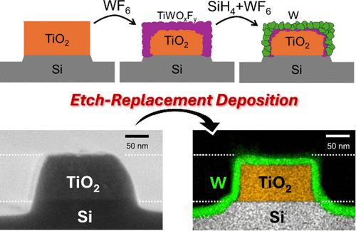
Thin film deposition and etching are two of the most widely used chemical processes in semiconductor manufacturing, and they are commonly carried out in distinct processing steps. In this work, we investigate low-temperature (250 °C) surface reactions that occur when a TiO2 surface undergoes chemical vapor etching, while at the same time, a layer of W metal is deposited at the location where the TiO2 was etched. The W deposition is performed using SiH4/WF6 exposures in an atomic layer deposition (ALD) sequence, where the WF6 provides a dual function as a precursor for W ALD and a reactant for TiO2 etching. Exposing TiO2 to WF6 leads to the formation of a mixed TiWOxFy surface layer that can be volatilized (i.e., etched) by further WF6 exposure. However, exposing the TiWOxFy to SiH4 promotes surface reduction so that subsequent WF6 exposure promotes W deposition. Introducing a controlled partial pressure of SiH4 in a SiH4/WF6 ALD sequence allows etching of TiO2 to continue but also promotes simultaneous W ALD so that the deposition and etch reactions “compete” for available WF6. Notably, the resulting W layer is formed at the location originally occupied by TiO2, thereby demonstrating “etch-replacement deposition.” In this case, the etch reactants are able to diffuse through the deposited W layer allowing more than 15 nm of TiO2 etching and 20 nm of W deposition. The results presented here provide insights into the interactions between deposition and etching reaction mechanisms, creating new opportunities for integrated atomic layer processing.
期刊介绍:
ACS Applied Polymer Materials is an interdisciplinary journal publishing original research covering all aspects of engineering, chemistry, physics, and biology relevant to applications of polymers.
The journal is devoted to reports of new and original experimental and theoretical research of an applied nature that integrates fundamental knowledge in the areas of materials, engineering, physics, bioscience, polymer science and chemistry into important polymer applications. The journal is specifically interested in work that addresses relationships among structure, processing, morphology, chemistry, properties, and function as well as work that provide insights into mechanisms critical to the performance of the polymer for applications.