通过原位诱导剪切应力调整三维打印 PVDF-MoS2 纳米复合材料的压电特性

IF 5.3 2区 材料科学 Q2 MATERIALS SCIENCE, MULTIDISCIPLINARY
Rifat Hasan Rupom, Md Nurul Islam, Zoriana Demchuk, Rigoberto Advincula, Narendra B. Dahotre, Yijie Jiang, Wonbong Choi
{"title":"通过原位诱导剪切应力调整三维打印 PVDF-MoS2 纳米复合材料的压电特性","authors":"Rifat Hasan Rupom, Md Nurul Islam, Zoriana Demchuk, Rigoberto Advincula, Narendra B. Dahotre, Yijie Jiang, Wonbong Choi","doi":"10.1021/acsanm.4c03695","DOIUrl":null,"url":null,"abstract":"3D printing of unique structures with tunable properties offers significant advantages in the fabrication of complex and customized electronic devices. This study introduces a process-microstructure–property-guided manufacturing route to fabricate PVDF-2D MoS<sub>2</sub> piezoelectric nanocomposites with tunable piezoelectric properties without having a postprocess. We control PVDF’s microstructure through direct ink writing (DIW) 3D printing while tuning PVDF-MoS<sub>2</sub> interfacial strain by controlling rheology and 3D printing parameters, such as nozzle size and printing speed. Our approach demonstrates tunable piezoelectricity in PVDF-MoS<sub>2</sub>, achieving a 15-fold increase in the piezoelectric coefficient (d<sub>33</sub>) at a printing-induced shear stress of 6685 Pa. This enhancement arises from the electrostatic interactions between PVDF and MoS<sub>2</sub> and the filler distribution and alignment caused by the in situ shear stress in 3D printing, as confirmed by XPS and Raman mapping analyses. Our findings advance the understanding of piezoelectric mechanisms in PVDF-based nanocomposites, laying the foundation for 3D printing of piezoelectric sensors in wearable device applications with enhanced performance and customization capabilities.","PeriodicalId":6,"journal":{"name":"ACS Applied Nano Materials","volume":null,"pages":null},"PeriodicalIF":5.3000,"publicationDate":"2024-09-19","publicationTypes":"Journal Article","fieldsOfStudy":null,"isOpenAccess":false,"openAccessPdf":"","citationCount":"0","resultStr":"{\"title\":\"Tailoring Piezoelectricity of 3D Printing PVDF-MoS2 Nanocomposite via In Situ Induced Shear Stress\",\"authors\":\"Rifat Hasan Rupom, Md Nurul Islam, Zoriana Demchuk, Rigoberto Advincula, Narendra B. Dahotre, Yijie Jiang, Wonbong Choi\",\"doi\":\"10.1021/acsanm.4c03695\",\"DOIUrl\":null,\"url\":null,\"abstract\":\"3D printing of unique structures with tunable properties offers significant advantages in the fabrication of complex and customized electronic devices. This study introduces a process-microstructure–property-guided manufacturing route to fabricate PVDF-2D MoS<sub>2</sub> piezoelectric nanocomposites with tunable piezoelectric properties without having a postprocess. We control PVDF’s microstructure through direct ink writing (DIW) 3D printing while tuning PVDF-MoS<sub>2</sub> interfacial strain by controlling rheology and 3D printing parameters, such as nozzle size and printing speed. Our approach demonstrates tunable piezoelectricity in PVDF-MoS<sub>2</sub>, achieving a 15-fold increase in the piezoelectric coefficient (d<sub>33</sub>) at a printing-induced shear stress of 6685 Pa. This enhancement arises from the electrostatic interactions between PVDF and MoS<sub>2</sub> and the filler distribution and alignment caused by the in situ shear stress in 3D printing, as confirmed by XPS and Raman mapping analyses. Our findings advance the understanding of piezoelectric mechanisms in PVDF-based nanocomposites, laying the foundation for 3D printing of piezoelectric sensors in wearable device applications with enhanced performance and customization capabilities.\",\"PeriodicalId\":6,\"journal\":{\"name\":\"ACS Applied Nano Materials\",\"volume\":null,\"pages\":null},\"PeriodicalIF\":5.3000,\"publicationDate\":\"2024-09-19\",\"publicationTypes\":\"Journal Article\",\"fieldsOfStudy\":null,\"isOpenAccess\":false,\"openAccessPdf\":\"\",\"citationCount\":\"0\",\"resultStr\":null,\"platform\":\"Semanticscholar\",\"paperid\":null,\"PeriodicalName\":\"ACS Applied Nano Materials\",\"FirstCategoryId\":\"88\",\"ListUrlMain\":\"https://doi.org/10.1021/acsanm.4c03695\",\"RegionNum\":2,\"RegionCategory\":\"材料科学\",\"ArticlePicture\":[],\"TitleCN\":null,\"AbstractTextCN\":null,\"PMCID\":null,\"EPubDate\":\"\",\"PubModel\":\"\",\"JCR\":\"Q2\",\"JCRName\":\"MATERIALS SCIENCE, MULTIDISCIPLINARY\",\"Score\":null,\"Total\":0}","platform":"Semanticscholar","paperid":null,"PeriodicalName":"ACS Applied Nano Materials","FirstCategoryId":"88","ListUrlMain":"https://doi.org/10.1021/acsanm.4c03695","RegionNum":2,"RegionCategory":"材料科学","ArticlePicture":[],"TitleCN":null,"AbstractTextCN":null,"PMCID":null,"EPubDate":"","PubModel":"","JCR":"Q2","JCRName":"MATERIALS SCIENCE, MULTIDISCIPLINARY","Score":null,"Total":0}
引用次数: 0

摘要

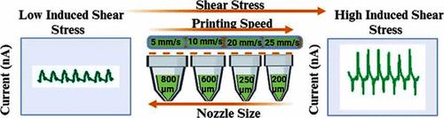
三维打印具有可调特性的独特结构为制造复杂的定制电子设备提供了显著优势。本研究介绍了一种工艺-微结构-特性引导的制造路线,无需后处理即可制造出具有可调压电特性的 PVDF-2D MoS2 压电纳米复合材料。我们通过直接墨水写入(DIW)三维打印技术控制 PVDF 的微观结构,同时通过控制流变学和三维打印参数(如喷嘴尺寸和打印速度)来调整 PVDF-MoS2 的界面应变。我们的方法证明了 PVDF-MoS2 的可调压电性,在 6685 Pa 的打印诱导剪切应力下,压电系数(d33)增加了 15 倍。这种增强源于 PVDF 和 MoS2 之间的静电相互作用,以及三维打印中原位剪切应力引起的填料分布和排列,XPS 和拉曼图谱分析证实了这一点。我们的研究结果加深了人们对基于 PVDF 的纳米复合材料中压电机制的理解,为可穿戴设备应用中压电传感器的三维打印奠定了基础,并提高了性能和定制能力。
本文章由计算机程序翻译,如有差异,请以英文原文为准。

Tailoring Piezoelectricity of 3D Printing PVDF-MoS2 Nanocomposite via In Situ Induced Shear Stress

Tailoring Piezoelectricity of 3D Printing PVDF-MoS2 Nanocomposite via In Situ Induced Shear Stress
3D printing of unique structures with tunable properties offers significant advantages in the fabrication of complex and customized electronic devices. This study introduces a process-microstructure–property-guided manufacturing route to fabricate PVDF-2D MoS2 piezoelectric nanocomposites with tunable piezoelectric properties without having a postprocess. We control PVDF’s microstructure through direct ink writing (DIW) 3D printing while tuning PVDF-MoS2 interfacial strain by controlling rheology and 3D printing parameters, such as nozzle size and printing speed. Our approach demonstrates tunable piezoelectricity in PVDF-MoS2, achieving a 15-fold increase in the piezoelectric coefficient (d33) at a printing-induced shear stress of 6685 Pa. This enhancement arises from the electrostatic interactions between PVDF and MoS2 and the filler distribution and alignment caused by the in situ shear stress in 3D printing, as confirmed by XPS and Raman mapping analyses. Our findings advance the understanding of piezoelectric mechanisms in PVDF-based nanocomposites, laying the foundation for 3D printing of piezoelectric sensors in wearable device applications with enhanced performance and customization capabilities.
求助全文
通过发布文献求助,成功后即可免费获取论文全文。 去求助
来源期刊
CiteScore
8.30
自引率
3.40%
发文量
1601
期刊介绍: ACS Applied Nano Materials is an interdisciplinary journal publishing original research covering all aspects of engineering, chemistry, physics and biology relevant to applications of nanomaterials. The journal is devoted to reports of new and original experimental and theoretical research of an applied nature that integrate knowledge in the areas of materials, engineering, physics, bioscience, and chemistry into important applications of nanomaterials.
×
引用
GB/T 7714-2015
复制
MLA
复制
APA
复制
导出至
BibTeX EndNote RefMan NoteFirst NoteExpress
×
提示
您的信息不完整,为了账户安全,请先补充。
现在去补充
×
提示
您因"违规操作"
具体请查看互助需知
我知道了
×
提示
确定
请完成安全验证×
copy
已复制链接
快去分享给好友吧!
我知道了
右上角分享
点击右上角分享
0
联系我们:info@booksci.cn Book学术提供免费学术资源搜索服务,方便国内外学者检索中英文文献。致力于提供最便捷和优质的服务体验。 Copyright © 2023 布克学术 All rights reserved.
京ICP备2023020795号-1
ghs 京公网安备 11010802042870号
Book学术文献互助
Book学术文献互助群
群 号:481959085
Book学术官方微信