Yang Wang , Ziyu Liu , Yabin Sun , Lin Chen , Qingqing Sun
{"title":"蚀刻出具有光滑侧壁和优异选择率的纳米 TSV,用于背面输电网络","authors":"Yang Wang , Ziyu Liu , Yabin Sun , Lin Chen , Qingqing Sun","doi":"10.1016/j.mee.2024.112265","DOIUrl":null,"url":null,"abstract":"<div><p>Backside Power Delivery Network (BSPDN) is a crucial technology for integrated circuits at sub-3 nm technology nodes. The primary challenge resides in utilizing nano through silicon via (nano-TSV) to establish connections between the backside power network and buried power rails, thereby facilitating transistor powering. The key technology is to ensure a smooth sidewall morphology and prevent damage to buried power rails (BPR) due to over-etching. In this study, non-Bosch and Bosch techniques are compared using simulation. The results demonstrate that while the non-Bosch technique yields smooth sidewalls, it inevitably leads to over-etching, whereas Bosch effectively avoids over-etching. The etching of scallop-free nano-TSV is achieved by optimizing the Bosch process, which involves the use of inductively coupled plasma (ICP). Finally, metal filling of nano-TSV is successfully achieved. Thus, the nano-TSV etching method is established as viable for BSPDN.</p></div>","PeriodicalId":18557,"journal":{"name":"Microelectronic Engineering","volume":"295 ","pages":"Article 112265"},"PeriodicalIF":3.1000,"publicationDate":"2024-09-05","publicationTypes":"Journal Article","fieldsOfStudy":null,"isOpenAccess":false,"openAccessPdf":"","citationCount":"0","resultStr":"{\"title\":\"Etch of nano-TSV with smooth sidewall and excellent selection ratio for backside power delivery network\",\"authors\":\"Yang Wang , Ziyu Liu , Yabin Sun , Lin Chen , Qingqing Sun\",\"doi\":\"10.1016/j.mee.2024.112265\",\"DOIUrl\":null,\"url\":null,\"abstract\":\"<div><p>Backside Power Delivery Network (BSPDN) is a crucial technology for integrated circuits at sub-3 nm technology nodes. The primary challenge resides in utilizing nano through silicon via (nano-TSV) to establish connections between the backside power network and buried power rails, thereby facilitating transistor powering. The key technology is to ensure a smooth sidewall morphology and prevent damage to buried power rails (BPR) due to over-etching. In this study, non-Bosch and Bosch techniques are compared using simulation. The results demonstrate that while the non-Bosch technique yields smooth sidewalls, it inevitably leads to over-etching, whereas Bosch effectively avoids over-etching. The etching of scallop-free nano-TSV is achieved by optimizing the Bosch process, which involves the use of inductively coupled plasma (ICP). Finally, metal filling of nano-TSV is successfully achieved. Thus, the nano-TSV etching method is established as viable for BSPDN.</p></div>\",\"PeriodicalId\":18557,\"journal\":{\"name\":\"Microelectronic Engineering\",\"volume\":\"295 \",\"pages\":\"Article 112265\"},\"PeriodicalIF\":3.1000,\"publicationDate\":\"2024-09-05\",\"publicationTypes\":\"Journal Article\",\"fieldsOfStudy\":null,\"isOpenAccess\":false,\"openAccessPdf\":\"\",\"citationCount\":\"0\",\"resultStr\":null,\"platform\":\"Semanticscholar\",\"paperid\":null,\"PeriodicalName\":\"Microelectronic Engineering\",\"FirstCategoryId\":\"5\",\"ListUrlMain\":\"https://www.sciencedirect.com/science/article/pii/S0167931724001345\",\"RegionNum\":4,\"RegionCategory\":\"工程技术\",\"ArticlePicture\":[],\"TitleCN\":null,\"AbstractTextCN\":null,\"PMCID\":null,\"EPubDate\":\"\",\"PubModel\":\"\",\"JCR\":\"Q2\",\"JCRName\":\"ENGINEERING, ELECTRICAL & ELECTRONIC\",\"Score\":null,\"Total\":0}","platform":"Semanticscholar","paperid":null,"PeriodicalName":"Microelectronic Engineering","FirstCategoryId":"5","ListUrlMain":"https://www.sciencedirect.com/science/article/pii/S0167931724001345","RegionNum":4,"RegionCategory":"工程技术","ArticlePicture":[],"TitleCN":null,"AbstractTextCN":null,"PMCID":null,"EPubDate":"","PubModel":"","JCR":"Q2","JCRName":"ENGINEERING, ELECTRICAL & ELECTRONIC","Score":null,"Total":0}
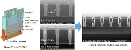
Etch of nano-TSV with smooth sidewall and excellent selection ratio for backside power delivery network
Backside Power Delivery Network (BSPDN) is a crucial technology for integrated circuits at sub-3 nm technology nodes. The primary challenge resides in utilizing nano through silicon via (nano-TSV) to establish connections between the backside power network and buried power rails, thereby facilitating transistor powering. The key technology is to ensure a smooth sidewall morphology and prevent damage to buried power rails (BPR) due to over-etching. In this study, non-Bosch and Bosch techniques are compared using simulation. The results demonstrate that while the non-Bosch technique yields smooth sidewalls, it inevitably leads to over-etching, whereas Bosch effectively avoids over-etching. The etching of scallop-free nano-TSV is achieved by optimizing the Bosch process, which involves the use of inductively coupled plasma (ICP). Finally, metal filling of nano-TSV is successfully achieved. Thus, the nano-TSV etching method is established as viable for BSPDN.
期刊介绍:
Microelectronic Engineering is the premier nanoprocessing, and nanotechnology journal focusing on fabrication of electronic, photonic, bioelectronic, electromechanic and fluidic devices and systems, and their applications in the broad areas of electronics, photonics, energy, life sciences, and environment. It covers also the expanding interdisciplinary field of "more than Moore" and "beyond Moore" integrated nanoelectronics / photonics and micro-/nano-/bio-systems. Through its unique mixture of peer-reviewed articles, reviews, accelerated publications, short and Technical notes, and the latest research news on key developments, Microelectronic Engineering provides comprehensive coverage of this exciting, interdisciplinary and dynamic new field for researchers in academia and professionals in industry.

 求助内容:
求助内容: 应助结果提醒方式:


