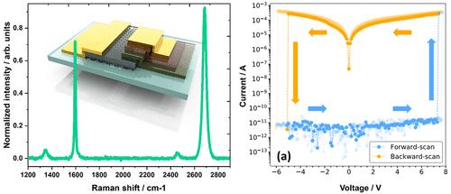
在蓝宝石晶片上直接生长单层石墨烯电极的晶体管

IF 4.3 3区 材料科学 Q1 ENGINEERING, ELECTRICAL & ELECTRONIC
Zhichao Weng, Robert Wallis, Bryan Wingfield, Paul Evans, Piotr Baginski, Jaspreet Kainth, Andrey E. Nikolaenko, Lok Yi Lee, Joanna Baginska, William P. Gillin, Ivor Guiney, Colin J. Humphreys, Oliver Fenwick
{"title":"在蓝宝石晶片上直接生长单层石墨烯电极的晶体管","authors":"Zhichao Weng, Robert Wallis, Bryan Wingfield, Paul Evans, Piotr Baginski, Jaspreet Kainth, Andrey E. Nikolaenko, Lok Yi Lee, Joanna Baginska, William P. Gillin, Ivor Guiney, Colin J. Humphreys, Oliver Fenwick","doi":"10.1021/acsaelm.4c01208","DOIUrl":null,"url":null,"abstract":"The development of the memristor has generated significant interest due to its non-volatility, simple structure, and low power consumption. Memristors based on graphene offer atomic monolayer thickness, flexibility, and uniformity and have attracted attention as a promising alternative to contemporary field-effect transistor (FET) technology in applications such as logic and memory devices, achieving higher integration density and lower power consumption. The use of graphene as electrodes in memristors could also increase robustness against degradation mechanisms, including oxygen vacancy diffusion to the electrode and unwanted metal ion diffusion. However, to realize this technological transformation, it is necessary to establish a scalable, robust, and cost-effective device fabrication process. Here we report the direct growth of high-quality monolayer graphene on sapphire wafers in a mass-producible, contamination-free, and transfer-free manner, using a commercially available metal–organic chemical vapor deposition (MOCVD) system. By taking advantage of this approach, graphene-electrode based memristors are developed, and all the processes used in the device fabrication incorporating graphene electrodes can be performed at wafer scale. The graphene electrode-based memristor demonstrates promising characteristics in terms of endurance, retention, and ON/OFF ratio. This work presents a possible and viable route to achieving robust graphene-based memristors in a commercially and technologically sustainable manner, paving the way for the realization of more powerful and compact integrated graphene electronics in the future.","PeriodicalId":3,"journal":{"name":"ACS Applied Electronic Materials","volume":"29 1","pages":""},"PeriodicalIF":4.3000,"publicationDate":"2024-09-16","publicationTypes":"Journal Article","fieldsOfStudy":null,"isOpenAccess":false,"openAccessPdf":"","citationCount":"0","resultStr":"{\"title\":\"Memristors with Monolayer Graphene Electrodes Grown Directly on Sapphire Wafers\",\"authors\":\"Zhichao Weng, Robert Wallis, Bryan Wingfield, Paul Evans, Piotr Baginski, Jaspreet Kainth, Andrey E. Nikolaenko, Lok Yi Lee, Joanna Baginska, William P. Gillin, Ivor Guiney, Colin J. Humphreys, Oliver Fenwick\",\"doi\":\"10.1021/acsaelm.4c01208\",\"DOIUrl\":null,\"url\":null,\"abstract\":\"The development of the memristor has generated significant interest due to its non-volatility, simple structure, and low power consumption. Memristors based on graphene offer atomic monolayer thickness, flexibility, and uniformity and have attracted attention as a promising alternative to contemporary field-effect transistor (FET) technology in applications such as logic and memory devices, achieving higher integration density and lower power consumption. The use of graphene as electrodes in memristors could also increase robustness against degradation mechanisms, including oxygen vacancy diffusion to the electrode and unwanted metal ion diffusion. However, to realize this technological transformation, it is necessary to establish a scalable, robust, and cost-effective device fabrication process. Here we report the direct growth of high-quality monolayer graphene on sapphire wafers in a mass-producible, contamination-free, and transfer-free manner, using a commercially available metal–organic chemical vapor deposition (MOCVD) system. By taking advantage of this approach, graphene-electrode based memristors are developed, and all the processes used in the device fabrication incorporating graphene electrodes can be performed at wafer scale. The graphene electrode-based memristor demonstrates promising characteristics in terms of endurance, retention, and ON/OFF ratio. This work presents a possible and viable route to achieving robust graphene-based memristors in a commercially and technologically sustainable manner, paving the way for the realization of more powerful and compact integrated graphene electronics in the future.\",\"PeriodicalId\":3,\"journal\":{\"name\":\"ACS Applied Electronic Materials\",\"volume\":\"29 1\",\"pages\":\"\"},\"PeriodicalIF\":4.3000,\"publicationDate\":\"2024-09-16\",\"publicationTypes\":\"Journal Article\",\"fieldsOfStudy\":null,\"isOpenAccess\":false,\"openAccessPdf\":\"\",\"citationCount\":\"0\",\"resultStr\":null,\"platform\":\"Semanticscholar\",\"paperid\":null,\"PeriodicalName\":\"ACS Applied Electronic Materials\",\"FirstCategoryId\":\"88\",\"ListUrlMain\":\"https://doi.org/10.1021/acsaelm.4c01208\",\"RegionNum\":3,\"RegionCategory\":\"材料科学\",\"ArticlePicture\":[],\"TitleCN\":null,\"AbstractTextCN\":null,\"PMCID\":null,\"EPubDate\":\"\",\"PubModel\":\"\",\"JCR\":\"Q1\",\"JCRName\":\"ENGINEERING, ELECTRICAL & ELECTRONIC\",\"Score\":null,\"Total\":0}","platform":"Semanticscholar","paperid":null,"PeriodicalName":"ACS Applied Electronic Materials","FirstCategoryId":"88","ListUrlMain":"https://doi.org/10.1021/acsaelm.4c01208","RegionNum":3,"RegionCategory":"材料科学","ArticlePicture":[],"TitleCN":null,"AbstractTextCN":null,"PMCID":null,"EPubDate":"","PubModel":"","JCR":"Q1","JCRName":"ENGINEERING, ELECTRICAL & ELECTRONIC","Score":null,"Total":0}
引用次数: 0

摘要

由于忆阻器具有不易挥发、结构简单和功耗低等特点,它的开发引起了人们的极大兴趣。基于石墨烯的忆阻器具有原子单层厚度、灵活性和均匀性,作为当代场效应晶体管(FET)技术在逻辑和存储设备等应用中的一种有前途的替代技术,它能实现更高的集成密度和更低的功耗,因而备受关注。在忆阻器中使用石墨烯作为电极,还能提高抗降解机制的稳健性,包括氧空位向电极的扩散和不需要的金属离子扩散。然而,要实现这一技术变革,必须建立一种可扩展、稳健且具有成本效益的器件制造工艺。在此,我们报告了利用市售的金属有机化学气相沉积(MOCVD)系统,以可大规模生产、无污染和无转移的方式在蓝宝石晶片上直接生长高质量单层石墨烯的情况。利用这种方法,我们开发出了基于石墨烯电极的忆阻器,并且可以在晶圆规模上完成包含石墨烯电极的器件制造过程中使用的所有工艺。基于石墨烯电极的忆阻器在耐久性、保持力和导通/关断比方面都表现出良好的特性。这项工作为以商业和技术上可持续的方式实现稳健的石墨烯基忆阻器提供了一条可行的途径,为未来实现功能更强大、结构更紧凑的集成石墨烯电子器件铺平了道路。
本文章由计算机程序翻译,如有差异,请以英文原文为准。

Memristors with Monolayer Graphene Electrodes Grown Directly on Sapphire Wafers

Memristors with Monolayer Graphene Electrodes Grown Directly on Sapphire Wafers
The development of the memristor has generated significant interest due to its non-volatility, simple structure, and low power consumption. Memristors based on graphene offer atomic monolayer thickness, flexibility, and uniformity and have attracted attention as a promising alternative to contemporary field-effect transistor (FET) technology in applications such as logic and memory devices, achieving higher integration density and lower power consumption. The use of graphene as electrodes in memristors could also increase robustness against degradation mechanisms, including oxygen vacancy diffusion to the electrode and unwanted metal ion diffusion. However, to realize this technological transformation, it is necessary to establish a scalable, robust, and cost-effective device fabrication process. Here we report the direct growth of high-quality monolayer graphene on sapphire wafers in a mass-producible, contamination-free, and transfer-free manner, using a commercially available metal–organic chemical vapor deposition (MOCVD) system. By taking advantage of this approach, graphene-electrode based memristors are developed, and all the processes used in the device fabrication incorporating graphene electrodes can be performed at wafer scale. The graphene electrode-based memristor demonstrates promising characteristics in terms of endurance, retention, and ON/OFF ratio. This work presents a possible and viable route to achieving robust graphene-based memristors in a commercially and technologically sustainable manner, paving the way for the realization of more powerful and compact integrated graphene electronics in the future.
求助全文
通过发布文献求助,成功后即可免费获取论文全文。 去求助
来源期刊
CiteScore
7.20
自引率
4.30%
发文量
567
期刊介绍: ACS Applied Electronic Materials is an interdisciplinary journal publishing original research covering all aspects of electronic materials. The journal is devoted to reports of new and original experimental and theoretical research of an applied nature that integrate knowledge in the areas of materials science, engineering, optics, physics, and chemistry into important applications of electronic materials. Sample research topics that span the journal's scope are inorganic, organic, ionic and polymeric materials with properties that include conducting, semiconducting, superconducting, insulating, dielectric, magnetic, optoelectronic, piezoelectric, ferroelectric and thermoelectric. Indexed/​Abstracted: Web of Science SCIE Scopus CAS INSPEC Portico
×
引用
GB/T 7714-2015
复制
MLA
复制
APA
复制
导出至
BibTeX EndNote RefMan NoteFirst NoteExpress
×
提示
您的信息不完整,为了账户安全,请先补充。
现在去补充
×
提示
您因"违规操作"
具体请查看互助需知
我知道了
×
提示
确定
请完成安全验证×
copy
已复制链接
快去分享给好友吧!
我知道了
右上角分享
点击右上角分享
0
联系我们:info@booksci.cn Book学术提供免费学术资源搜索服务,方便国内外学者检索中英文文献。致力于提供最便捷和优质的服务体验。 Copyright © 2023 布克学术 All rights reserved.
京ICP备2023020795号-1
ghs 京公网安备 11010802042870号
Book学术文献互助
Book学术文献互助群
群 号:481959085
Book学术官方微信