β-Ga2O3晶体中的弯形双边界
IF 3.2
2区 化学
Q2 CHEMISTRY, MULTIDISCIPLINARY
引用次数: 0
摘要
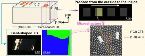
孪晶边界(TB)作为一种二维缺陷,会限制晶体材料的尺寸,降低单晶产量,影响后续器件的性能。对于β-Ga2O3来说,它是最有前途的超宽带隙半导体材料之一,但却受到孪晶问题的严重限制。本文发现并详细讨论了β-Ga2O3 体晶中具有弯曲状 TB 的非穿透孪晶结构。利用电子反向散射衍射(EBSD)和球面像差校正扫描透射电子显微镜(AC-STEM)成像技术,从(010)和(100)两个方向深入研究了β-Ga2O3 中弯曲形 TB 的取向差异和原子尺度上的微观结构。结果表明,弯曲状 TB 为 180° TB,由非相干 TB(ITB)和(100)相干 TB(CTB)组合而成。ITB 可以进一步表示为 (1̅02)-CTB 和 (100)-CTB 的组合。根据 TB 形成能(ETB)和晶体生长动力学,阐明了β-Ga2O3 中弯曲状 TB 的形成机制。该研究揭示了弯曲状 TB 的微观结构和形成机制,丰富了有关 β-Ga2O3 晶体缺陷的研究。本文章由计算机程序翻译,如有差异,请以英文原文为准。
Bent-Shaped Twin Boundary in β-Ga2O3 Crystals
Twin boundary (TB) as a two-dimensional defect will constrain the size of the crystal material, reduce the yield of single crystals, and affect the performance of subsequent devices. For β-Ga2O3, it is one of the most promising ultrawide-band-gap semiconductor materials, which is severely limited by the twinning problem. In this paper, the unpenetrated twin structure with bent-shaped TB in the β-Ga2O3 bulk crystal was found and discussed in detail. The orientation difference and microstructure on the atomic scale of the bent-shaped TB in β-Ga2O3 have been intensively investigated from the (010) and (100) orientations using electron backscatter diffraction (EBSD) and spherical aberration-corrected scanning transmission electron microscopy (AC-STEM) imaging techniques. The results indicate that the bent-shaped TB is 180° TB, formed by the combination of incoherent TB (ITB) and (100)-coherent TB (CTB). The ITB can be further represented as a combination of (1̅02)-CTB and (100)-CTB. The formation mechanism of the bent-shaped TB in β-Ga2O3 is elucidated based on the TB formation energy (ETB) and crystal growth kinetics. This study reveals the microstructure and formation mechanism of bent-shaped TB and enriches the work on crystal defects in β-Ga2O3.
求助全文
通过发布文献求助,成功后即可免费获取论文全文。
去求助
来源期刊

Crystal Growth & Design
化学-材料科学:综合
CiteScore
6.30
自引率
10.50%
发文量
650
审稿时长
1.9 months
期刊介绍:
The aim of Crystal Growth & Design is to stimulate crossfertilization of knowledge among scientists and engineers working in the fields of crystal growth, crystal engineering, and the industrial application of crystalline materials.
Crystal Growth & Design publishes theoretical and experimental studies of the physical, chemical, and biological phenomena and processes related to the design, growth, and application of crystalline materials. Synergistic approaches originating from different disciplines and technologies and integrating the fields of crystal growth, crystal engineering, intermolecular interactions, and industrial application are encouraged.
 求助内容:
求助内容: 应助结果提醒方式:


