纳米级 ScGaN 的分子束外延生长与表征

IF 3.2 2区 化学 Q2 CHEMISTRY, MULTIDISCIPLINARY
Mohammad Fazel Vafadar, Milad Fathabadi, Songrui Zhao
{"title":"纳米级 ScGaN 的分子束外延生长与表征","authors":"Mohammad Fazel Vafadar, Milad Fathabadi, Songrui Zhao","doi":"10.1021/acs.cgd.4c00814","DOIUrl":null,"url":null,"abstract":"Low-dimensional semiconductor materials, including nanowires, have been an attractive platform for cutting-edge semiconductor device development. On the other hand, scandium (Sc) containing III-nitrides (Sc–III-nitrides) is an emerging material system, offering not only novel ferroelectric devices but also potentially multifunctional devices in a single-material platform. In this study, we investigate nanoscale Sc<sub><i>x</i></sub>Ga<sub>1–<i>x</i></sub>N (ScGaN) hosted in GaN nanowires grown by molecular beam epitaxy on Si substrate. The major findings are (1) Within each ScGaN insert layer, the Sc content is not uniform as indicated by transmission electron microscopy studies, suggesting the formation of ScGaN nanoclusters with different Sc contents; (2) ScGaN shell is formed spontaneously; and (3) Zincblende phase is observed in the ScGaN insert layers although the estimated average Sc content is only around <i>x</i> = 0.16. The possible mechanisms related to these findings are also discussed. These unveiled correlated epitaxial and structural properties could help in the development of Sc–III-nitride nanowire devices.","PeriodicalId":34,"journal":{"name":"Crystal Growth & Design","volume":null,"pages":null},"PeriodicalIF":3.2000,"publicationDate":"2024-09-15","publicationTypes":"Journal Article","fieldsOfStudy":null,"isOpenAccess":false,"openAccessPdf":"","citationCount":"0","resultStr":"{\"title\":\"Molecular Beam Epitaxial Growth and Characterization of Nanoscale ScGaN\",\"authors\":\"Mohammad Fazel Vafadar, Milad Fathabadi, Songrui Zhao\",\"doi\":\"10.1021/acs.cgd.4c00814\",\"DOIUrl\":null,\"url\":null,\"abstract\":\"Low-dimensional semiconductor materials, including nanowires, have been an attractive platform for cutting-edge semiconductor device development. On the other hand, scandium (Sc) containing III-nitrides (Sc–III-nitrides) is an emerging material system, offering not only novel ferroelectric devices but also potentially multifunctional devices in a single-material platform. In this study, we investigate nanoscale Sc<sub><i>x</i></sub>Ga<sub>1–<i>x</i></sub>N (ScGaN) hosted in GaN nanowires grown by molecular beam epitaxy on Si substrate. The major findings are (1) Within each ScGaN insert layer, the Sc content is not uniform as indicated by transmission electron microscopy studies, suggesting the formation of ScGaN nanoclusters with different Sc contents; (2) ScGaN shell is formed spontaneously; and (3) Zincblende phase is observed in the ScGaN insert layers although the estimated average Sc content is only around <i>x</i> = 0.16. The possible mechanisms related to these findings are also discussed. These unveiled correlated epitaxial and structural properties could help in the development of Sc–III-nitride nanowire devices.\",\"PeriodicalId\":34,\"journal\":{\"name\":\"Crystal Growth & Design\",\"volume\":null,\"pages\":null},\"PeriodicalIF\":3.2000,\"publicationDate\":\"2024-09-15\",\"publicationTypes\":\"Journal Article\",\"fieldsOfStudy\":null,\"isOpenAccess\":false,\"openAccessPdf\":\"\",\"citationCount\":\"0\",\"resultStr\":null,\"platform\":\"Semanticscholar\",\"paperid\":null,\"PeriodicalName\":\"Crystal Growth & Design\",\"FirstCategoryId\":\"92\",\"ListUrlMain\":\"https://doi.org/10.1021/acs.cgd.4c00814\",\"RegionNum\":2,\"RegionCategory\":\"化学\",\"ArticlePicture\":[],\"TitleCN\":null,\"AbstractTextCN\":null,\"PMCID\":null,\"EPubDate\":\"\",\"PubModel\":\"\",\"JCR\":\"Q2\",\"JCRName\":\"CHEMISTRY, MULTIDISCIPLINARY\",\"Score\":null,\"Total\":0}","platform":"Semanticscholar","paperid":null,"PeriodicalName":"Crystal Growth & Design","FirstCategoryId":"92","ListUrlMain":"https://doi.org/10.1021/acs.cgd.4c00814","RegionNum":2,"RegionCategory":"化学","ArticlePicture":[],"TitleCN":null,"AbstractTextCN":null,"PMCID":null,"EPubDate":"","PubModel":"","JCR":"Q2","JCRName":"CHEMISTRY, MULTIDISCIPLINARY","Score":null,"Total":0}
引用次数: 0

摘要

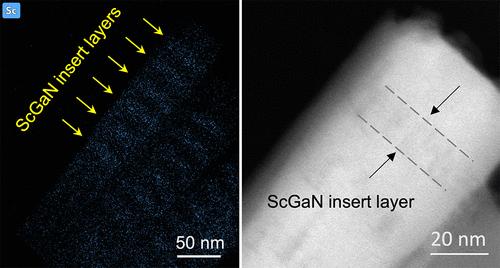
包括纳米线在内的低维半导体材料一直是开发尖端半导体器件的诱人平台。另一方面,含钪(Sc)的 III-氮化物(Sc-III-nitrides)是一种新兴的材料体系,它不仅能提供新型铁电器件,还可能在单一材料平台上提供多功能器件。在本研究中,我们研究了在硅衬底上通过分子束外延生长的 GaN 纳米线中寄存的纳米级 ScxGa1-xN (ScGaN)。主要发现有:(1)透射电子显微镜研究表明,在每个 ScGaN 插入层中,Sc 的含量并不均匀,这表明形成了具有不同 Sc 含量的 ScGaN 纳米簇;(2)ScGaN 壳是自发形成的;(3)尽管估计的平均 Sc 含量仅为 x = 0.16 左右,但在 ScGaN 插入层中观察到了锌帘石相。此外,还讨论了与这些发现相关的可能机制。这些揭示的相关外延和结构特性有助于开发 Sc-III 氮化物纳米线器件。
本文章由计算机程序翻译,如有差异,请以英文原文为准。

Molecular Beam Epitaxial Growth and Characterization of Nanoscale ScGaN

Molecular Beam Epitaxial Growth and Characterization of Nanoscale ScGaN
Low-dimensional semiconductor materials, including nanowires, have been an attractive platform for cutting-edge semiconductor device development. On the other hand, scandium (Sc) containing III-nitrides (Sc–III-nitrides) is an emerging material system, offering not only novel ferroelectric devices but also potentially multifunctional devices in a single-material platform. In this study, we investigate nanoscale ScxGa1–xN (ScGaN) hosted in GaN nanowires grown by molecular beam epitaxy on Si substrate. The major findings are (1) Within each ScGaN insert layer, the Sc content is not uniform as indicated by transmission electron microscopy studies, suggesting the formation of ScGaN nanoclusters with different Sc contents; (2) ScGaN shell is formed spontaneously; and (3) Zincblende phase is observed in the ScGaN insert layers although the estimated average Sc content is only around x = 0.16. The possible mechanisms related to these findings are also discussed. These unveiled correlated epitaxial and structural properties could help in the development of Sc–III-nitride nanowire devices.
求助全文
通过发布文献求助,成功后即可免费获取论文全文。 去求助
来源期刊
Crystal Growth & Design
Crystal Growth & Design 化学-材料科学:综合
CiteScore
6.30
自引率
10.50%
发文量
650
审稿时长
1.9 months
期刊介绍: The aim of Crystal Growth & Design is to stimulate crossfertilization of knowledge among scientists and engineers working in the fields of crystal growth, crystal engineering, and the industrial application of crystalline materials. Crystal Growth & Design publishes theoretical and experimental studies of the physical, chemical, and biological phenomena and processes related to the design, growth, and application of crystalline materials. Synergistic approaches originating from different disciplines and technologies and integrating the fields of crystal growth, crystal engineering, intermolecular interactions, and industrial application are encouraged.
×
引用
GB/T 7714-2015
复制
MLA
复制
APA
复制
导出至
BibTeX EndNote RefMan NoteFirst NoteExpress
×
提示
您的信息不完整,为了账户安全,请先补充。
现在去补充
×
提示
您因"违规操作"
具体请查看互助需知
我知道了
×
提示
确定
请完成安全验证×
copy
已复制链接
快去分享给好友吧!
我知道了
右上角分享
点击右上角分享
0
联系我们:info@booksci.cn Book学术提供免费学术资源搜索服务,方便国内外学者检索中英文文献。致力于提供最便捷和优质的服务体验。 Copyright © 2023 布克学术 All rights reserved.
京ICP备2023020795号-1
ghs 京公网安备 11010802042870号
Book学术文献互助
Book学术文献互助群
群 号:481959085
Book学术官方微信