Xiangyu Zhao, Hao Jiang, Jiamin Liu, Changqing Liu, Hui Deng, Renjie Zhou, Nicholas X. Fang, Shiyuan Liu* and Jinlong Zhu*,
{"title":"直接监测三维堆叠结构中所有层的纳米级变形","authors":"Xiangyu Zhao, Hao Jiang, Jiamin Liu, Changqing Liu, Hui Deng, Renjie Zhou, Nicholas X. Fang, Shiyuan Liu* and Jinlong Zhu*, ","doi":"10.1021/acsphotonics.4c0078410.1021/acsphotonics.4c00784","DOIUrl":null,"url":null,"abstract":"<p >Due to its high bandwidth, low latency, low power consumption, and compact size, three-dimensional (3D) integration of semiconductor chips holds the promise of boosting the performance of integrated circuit systems. However, the applications of 3D stacked structures are constrained by the surface deformation of each thin layer induced by thermal effects, vibration, gravity, and other environmental stresses. Therefore, ensuring the performance and reliability of 3D stacked structures necessitates the precise measurement of nanoscale deformation in each layer. Furthermore, the spacing between layers in 3D stacked structures using modern microelectronics and packaging technologies is exceedingly small, making it impossible to measure the deformation of all layers. Here, we present a novel optical endoscope that fuses a miniaturized interferometry array, a laser-fabricated microprobe, and a highly efficient profile reconstruction algorithm for the precise measurements of surface deformation across all layers in 3D stacked structures. Our method offers a potentially effective and noninvasive way to address the challenges associated with in-line deformation measurement across all layers in real 3D stacked wafers and chips.</p>","PeriodicalId":23,"journal":{"name":"ACS Photonics","volume":"11 9","pages":"3672–3679 3672–3679"},"PeriodicalIF":6.7000,"publicationDate":"2024-08-30","publicationTypes":"Journal Article","fieldsOfStudy":null,"isOpenAccess":false,"openAccessPdf":"","citationCount":"0","resultStr":"{\"title\":\"Direct Monitoring of Nanoscale Deformations across All Layers in Three-Dimensional Stacked Structures\",\"authors\":\"Xiangyu Zhao, Hao Jiang, Jiamin Liu, Changqing Liu, Hui Deng, Renjie Zhou, Nicholas X. Fang, Shiyuan Liu* and Jinlong Zhu*, \",\"doi\":\"10.1021/acsphotonics.4c0078410.1021/acsphotonics.4c00784\",\"DOIUrl\":null,\"url\":null,\"abstract\":\"<p >Due to its high bandwidth, low latency, low power consumption, and compact size, three-dimensional (3D) integration of semiconductor chips holds the promise of boosting the performance of integrated circuit systems. However, the applications of 3D stacked structures are constrained by the surface deformation of each thin layer induced by thermal effects, vibration, gravity, and other environmental stresses. Therefore, ensuring the performance and reliability of 3D stacked structures necessitates the precise measurement of nanoscale deformation in each layer. Furthermore, the spacing between layers in 3D stacked structures using modern microelectronics and packaging technologies is exceedingly small, making it impossible to measure the deformation of all layers. Here, we present a novel optical endoscope that fuses a miniaturized interferometry array, a laser-fabricated microprobe, and a highly efficient profile reconstruction algorithm for the precise measurements of surface deformation across all layers in 3D stacked structures. Our method offers a potentially effective and noninvasive way to address the challenges associated with in-line deformation measurement across all layers in real 3D stacked wafers and chips.</p>\",\"PeriodicalId\":23,\"journal\":{\"name\":\"ACS Photonics\",\"volume\":\"11 9\",\"pages\":\"3672–3679 3672–3679\"},\"PeriodicalIF\":6.7000,\"publicationDate\":\"2024-08-30\",\"publicationTypes\":\"Journal Article\",\"fieldsOfStudy\":null,\"isOpenAccess\":false,\"openAccessPdf\":\"\",\"citationCount\":\"0\",\"resultStr\":null,\"platform\":\"Semanticscholar\",\"paperid\":null,\"PeriodicalName\":\"ACS Photonics\",\"FirstCategoryId\":\"101\",\"ListUrlMain\":\"https://pubs.acs.org/doi/10.1021/acsphotonics.4c00784\",\"RegionNum\":1,\"RegionCategory\":\"物理与天体物理\",\"ArticlePicture\":[],\"TitleCN\":null,\"AbstractTextCN\":null,\"PMCID\":null,\"EPubDate\":\"\",\"PubModel\":\"\",\"JCR\":\"Q1\",\"JCRName\":\"MATERIALS SCIENCE, MULTIDISCIPLINARY\",\"Score\":null,\"Total\":0}","platform":"Semanticscholar","paperid":null,"PeriodicalName":"ACS Photonics","FirstCategoryId":"101","ListUrlMain":"https://pubs.acs.org/doi/10.1021/acsphotonics.4c00784","RegionNum":1,"RegionCategory":"物理与天体物理","ArticlePicture":[],"TitleCN":null,"AbstractTextCN":null,"PMCID":null,"EPubDate":"","PubModel":"","JCR":"Q1","JCRName":"MATERIALS SCIENCE, MULTIDISCIPLINARY","Score":null,"Total":0}
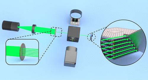
Direct Monitoring of Nanoscale Deformations across All Layers in Three-Dimensional Stacked Structures
Due to its high bandwidth, low latency, low power consumption, and compact size, three-dimensional (3D) integration of semiconductor chips holds the promise of boosting the performance of integrated circuit systems. However, the applications of 3D stacked structures are constrained by the surface deformation of each thin layer induced by thermal effects, vibration, gravity, and other environmental stresses. Therefore, ensuring the performance and reliability of 3D stacked structures necessitates the precise measurement of nanoscale deformation in each layer. Furthermore, the spacing between layers in 3D stacked structures using modern microelectronics and packaging technologies is exceedingly small, making it impossible to measure the deformation of all layers. Here, we present a novel optical endoscope that fuses a miniaturized interferometry array, a laser-fabricated microprobe, and a highly efficient profile reconstruction algorithm for the precise measurements of surface deformation across all layers in 3D stacked structures. Our method offers a potentially effective and noninvasive way to address the challenges associated with in-line deformation measurement across all layers in real 3D stacked wafers and chips.
期刊介绍:
Published as soon as accepted and summarized in monthly issues, ACS Photonics will publish Research Articles, Letters, Perspectives, and Reviews, to encompass the full scope of published research in this field.

 求助内容:
求助内容: 应助结果提醒方式:


