Abduelwhab B. Alwany, Belqees Hassan, Yahya Alajlani, Ali Alnakhlani, Rehab. A. Fouad
{"title":"分析薄膜厚度变化对 Ge15Se75Zn10 薄膜结构和光学特性的影响","authors":"Abduelwhab B. Alwany, Belqees Hassan, Yahya Alajlani, Ali Alnakhlani, Rehab. A. Fouad","doi":"10.1007/s10904-024-03325-8","DOIUrl":null,"url":null,"abstract":"<p>Ge<sub>15</sub>Se<sub>75</sub>Zn<sub>10</sub> thin films (TFs) with varying thicknesses were deposited onto glass substrates via vacuum evaporation. These TFs were subjected to comprehensive characterization through X-ray diffraction (XRD), Scanning Electron Microscopy (SEM), and optical spectroscopy. XRD analysis of the deposited Ge<sub>15</sub>Se<sub>75</sub>Zn<sub>10</sub> thin films at different thicknesses indicated that the 250 nm film exhibited an amorphous structure, while the 350 and 450 nm films exhibited crystalline phases, predominantly composed of GeSe and ZnSe. The crystalline sizes of these phases increased with film thickness, reaching 25 nm and 49 nm for ZnSe and GeSe, respectively, in the 450 nm film. SEM imaging revealed fine particles dispersed within an amorphous matrix in the 250 nm film, while erratic particle sizes and shapes were observed in the 350 nm film, with a more uniform distribution in thicker films. These SEM results provided complementary insights to the X-ray analysis. Optical properties were investigated by measuring transmittance T(λ) and reflectance R(λ). The optical band gap (E<sub>g</sub>) decreased with increasing film thickness, measuring 2.913 eV, 2.780 eV, and 2.83 eV for the 250 nm, 350 nm, and 450 nm films, respectively. Additionally, Urbach energy (E<sub>U</sub>), dielectric constant of high frequency (ε<sub>L</sub>), and charge carrier concentration increased with film thickness, while the energy of the single oscillator (E<sub>o</sub>) and dispersive energy (E<sub>d</sub>) decreased with increasing TFs thickness. These research findings offer valuable insights into the structural, morphological, and optical characteristics of Ge<sub>15</sub>Se<sub>75</sub>Zn<sub>10</sub> TFs, showcasing potential applications in optoelectronic devices and thin film technology. A systematic exploration of these thin films not only advances materials science and technology but also opens avenues for future research and development across diverse fields.</p>","PeriodicalId":639,"journal":{"name":"Journal of Inorganic and Organometallic Polymers and Materials","volume":"18 1","pages":""},"PeriodicalIF":3.9000,"publicationDate":"2024-08-14","publicationTypes":"Journal Article","fieldsOfStudy":null,"isOpenAccess":false,"openAccessPdf":"","citationCount":"0","resultStr":"{\"title\":\"Analyzing the Influence of Varying Film Thickness on the Structural and Optical Properties of Ge15Se75Zn10 Thin Films\",\"authors\":\"Abduelwhab B. Alwany, Belqees Hassan, Yahya Alajlani, Ali Alnakhlani, Rehab. A. Fouad\",\"doi\":\"10.1007/s10904-024-03325-8\",\"DOIUrl\":null,\"url\":null,\"abstract\":\"<p>Ge<sub>15</sub>Se<sub>75</sub>Zn<sub>10</sub> thin films (TFs) with varying thicknesses were deposited onto glass substrates via vacuum evaporation. These TFs were subjected to comprehensive characterization through X-ray diffraction (XRD), Scanning Electron Microscopy (SEM), and optical spectroscopy. XRD analysis of the deposited Ge<sub>15</sub>Se<sub>75</sub>Zn<sub>10</sub> thin films at different thicknesses indicated that the 250 nm film exhibited an amorphous structure, while the 350 and 450 nm films exhibited crystalline phases, predominantly composed of GeSe and ZnSe. The crystalline sizes of these phases increased with film thickness, reaching 25 nm and 49 nm for ZnSe and GeSe, respectively, in the 450 nm film. SEM imaging revealed fine particles dispersed within an amorphous matrix in the 250 nm film, while erratic particle sizes and shapes were observed in the 350 nm film, with a more uniform distribution in thicker films. These SEM results provided complementary insights to the X-ray analysis. Optical properties were investigated by measuring transmittance T(λ) and reflectance R(λ). The optical band gap (E<sub>g</sub>) decreased with increasing film thickness, measuring 2.913 eV, 2.780 eV, and 2.83 eV for the 250 nm, 350 nm, and 450 nm films, respectively. Additionally, Urbach energy (E<sub>U</sub>), dielectric constant of high frequency (ε<sub>L</sub>), and charge carrier concentration increased with film thickness, while the energy of the single oscillator (E<sub>o</sub>) and dispersive energy (E<sub>d</sub>) decreased with increasing TFs thickness. These research findings offer valuable insights into the structural, morphological, and optical characteristics of Ge<sub>15</sub>Se<sub>75</sub>Zn<sub>10</sub> TFs, showcasing potential applications in optoelectronic devices and thin film technology. A systematic exploration of these thin films not only advances materials science and technology but also opens avenues for future research and development across diverse fields.</p>\",\"PeriodicalId\":639,\"journal\":{\"name\":\"Journal of Inorganic and Organometallic Polymers and Materials\",\"volume\":\"18 1\",\"pages\":\"\"},\"PeriodicalIF\":3.9000,\"publicationDate\":\"2024-08-14\",\"publicationTypes\":\"Journal Article\",\"fieldsOfStudy\":null,\"isOpenAccess\":false,\"openAccessPdf\":\"\",\"citationCount\":\"0\",\"resultStr\":null,\"platform\":\"Semanticscholar\",\"paperid\":null,\"PeriodicalName\":\"Journal of Inorganic and Organometallic Polymers and Materials\",\"FirstCategoryId\":\"92\",\"ListUrlMain\":\"https://doi.org/10.1007/s10904-024-03325-8\",\"RegionNum\":3,\"RegionCategory\":\"化学\",\"ArticlePicture\":[],\"TitleCN\":null,\"AbstractTextCN\":null,\"PMCID\":null,\"EPubDate\":\"\",\"PubModel\":\"\",\"JCR\":\"Q2\",\"JCRName\":\"POLYMER SCIENCE\",\"Score\":null,\"Total\":0}","platform":"Semanticscholar","paperid":null,"PeriodicalName":"Journal of Inorganic and Organometallic Polymers and Materials","FirstCategoryId":"92","ListUrlMain":"https://doi.org/10.1007/s10904-024-03325-8","RegionNum":3,"RegionCategory":"化学","ArticlePicture":[],"TitleCN":null,"AbstractTextCN":null,"PMCID":null,"EPubDate":"","PubModel":"","JCR":"Q2","JCRName":"POLYMER SCIENCE","Score":null,"Total":0}
Analyzing the Influence of Varying Film Thickness on the Structural and Optical Properties of Ge15Se75Zn10 Thin Films
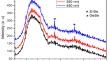
Ge15Se75Zn10 thin films (TFs) with varying thicknesses were deposited onto glass substrates via vacuum evaporation. These TFs were subjected to comprehensive characterization through X-ray diffraction (XRD), Scanning Electron Microscopy (SEM), and optical spectroscopy. XRD analysis of the deposited Ge15Se75Zn10 thin films at different thicknesses indicated that the 250 nm film exhibited an amorphous structure, while the 350 and 450 nm films exhibited crystalline phases, predominantly composed of GeSe and ZnSe. The crystalline sizes of these phases increased with film thickness, reaching 25 nm and 49 nm for ZnSe and GeSe, respectively, in the 450 nm film. SEM imaging revealed fine particles dispersed within an amorphous matrix in the 250 nm film, while erratic particle sizes and shapes were observed in the 350 nm film, with a more uniform distribution in thicker films. These SEM results provided complementary insights to the X-ray analysis. Optical properties were investigated by measuring transmittance T(λ) and reflectance R(λ). The optical band gap (Eg) decreased with increasing film thickness, measuring 2.913 eV, 2.780 eV, and 2.83 eV for the 250 nm, 350 nm, and 450 nm films, respectively. Additionally, Urbach energy (EU), dielectric constant of high frequency (εL), and charge carrier concentration increased with film thickness, while the energy of the single oscillator (Eo) and dispersive energy (Ed) decreased with increasing TFs thickness. These research findings offer valuable insights into the structural, morphological, and optical characteristics of Ge15Se75Zn10 TFs, showcasing potential applications in optoelectronic devices and thin film technology. A systematic exploration of these thin films not only advances materials science and technology but also opens avenues for future research and development across diverse fields.
期刊介绍:
Journal of Inorganic and Organometallic Polymers and Materials [JIOP or JIOPM] is a comprehensive resource for reports on the latest theoretical and experimental research. This bimonthly journal encompasses a broad range of synthetic and natural substances which contain main group, transition, and inner transition elements. The publication includes fully peer-reviewed original papers and shorter communications, as well as topical review papers that address the synthesis, characterization, evaluation, and phenomena of inorganic and organometallic polymers, materials, and supramolecular systems.
 求助内容:
求助内容: 应助结果提醒方式:


