V. N. Senthil Kumaran, M. Venkatesh, Azath Mubarakali, Abdulrahman Saad Alqahtani, P. Parthasarathy
{"title":"利用基于等离子体辅助分子束外延的超高真空沉积技术制造调制掺杂的 β-(AlxGa1-x)2O3/Ga2O3 三金属场效应晶体管并确定其特性","authors":"V. N. Senthil Kumaran, M. Venkatesh, Azath Mubarakali, Abdulrahman Saad Alqahtani, P. Parthasarathy","doi":"10.1007/s10854-024-13430-6","DOIUrl":null,"url":null,"abstract":"<p>This study investigates the design of MOD-FETs (modulation-doped field effect transistors) using β-Ga<sub>2</sub>O<sub>3</sub> as the substrate material. The main focus is on understanding the impact of self-heating on the alteration of mobility of electrons profile. This paper introduces a model that takes into account the influence on temperature and doping on the electron mobility in β-Ga<sub>2</sub>O<sub>3</sub>. Furthermore, it offers estimations for the conductivity of heat of β-Ga<sub>2</sub>O<sub>3</sub>, considering the influence of temperature and crystalline orientation. Furthermore, we showcase a practical example of modulation-doped β-(Al<sub>x</sub>Ga<sub>1-x</sub>)<sub>2</sub>O<sub>3</sub>/Ga<sub>2</sub>O<sub>3</sub> using a tri-metal FET where the energy level difference between the conduction bands and the presence of undesired channels in the barrier layer determines the maximum sheet carrier density in this structure. These channels enable the transfer of electrons from both the bottom and upper portions of the β-Ga<sub>2</sub>O<sub>3</sub> quantum well. Using modulation doping, the proposed structure exhibited an ultimate current drain of 250 mA/m, a peak conductivity of 40 ms/m, and a potential of 10.0 V at ambient temperature. The electrical characteristics of the TMG device were evaluated by comparing it to the double-metal gate (DMG) device using the Atlas Silvaco TCAD simulation for analysis of performance. The results indicate that, the suggested device exhibits greater efficiency in terms of conductivity, current gain cut-off frequency, and energy gain cut-off frequency as compared to DMG transistors. The measured electric field in this example is a consequence of using a Tri-Metal Gate architecture (TMG) to regulate the channel. The designed setup achieves peak frequency of 45.5/50.5 gigahertz with a gate length of 0.2 mm. This discovery highlights the potential of using the β-(Al<sub>x</sub>Ga<sub>1−x</sub>)<sub>2</sub>O<sub>3</sub>/Ga<sub>2</sub>O<sub>3</sub> with tri-metal FET architecture as a promising method for high-power radio frequency operations.</p>","PeriodicalId":646,"journal":{"name":"Journal of Materials Science: Materials in Electronics","volume":null,"pages":null},"PeriodicalIF":2.8000,"publicationDate":"2024-09-11","publicationTypes":"Journal Article","fieldsOfStudy":null,"isOpenAccess":false,"openAccessPdf":"","citationCount":"0","resultStr":"{\"title\":\"Fabrication and characterization of modulation-doped β-(AlxGa1−x)2O3/Ga2O3 tri-metal FET utilizing ultra-high vacuum deposition based on plasma-assisted molecular beam epitaxy\",\"authors\":\"V. N. Senthil Kumaran, M. Venkatesh, Azath Mubarakali, Abdulrahman Saad Alqahtani, P. Parthasarathy\",\"doi\":\"10.1007/s10854-024-13430-6\",\"DOIUrl\":null,\"url\":null,\"abstract\":\"<p>This study investigates the design of MOD-FETs (modulation-doped field effect transistors) using β-Ga<sub>2</sub>O<sub>3</sub> as the substrate material. The main focus is on understanding the impact of self-heating on the alteration of mobility of electrons profile. This paper introduces a model that takes into account the influence on temperature and doping on the electron mobility in β-Ga<sub>2</sub>O<sub>3</sub>. Furthermore, it offers estimations for the conductivity of heat of β-Ga<sub>2</sub>O<sub>3</sub>, considering the influence of temperature and crystalline orientation. Furthermore, we showcase a practical example of modulation-doped β-(Al<sub>x</sub>Ga<sub>1-x</sub>)<sub>2</sub>O<sub>3</sub>/Ga<sub>2</sub>O<sub>3</sub> using a tri-metal FET where the energy level difference between the conduction bands and the presence of undesired channels in the barrier layer determines the maximum sheet carrier density in this structure. These channels enable the transfer of electrons from both the bottom and upper portions of the β-Ga<sub>2</sub>O<sub>3</sub> quantum well. Using modulation doping, the proposed structure exhibited an ultimate current drain of 250 mA/m, a peak conductivity of 40 ms/m, and a potential of 10.0 V at ambient temperature. The electrical characteristics of the TMG device were evaluated by comparing it to the double-metal gate (DMG) device using the Atlas Silvaco TCAD simulation for analysis of performance. The results indicate that, the suggested device exhibits greater efficiency in terms of conductivity, current gain cut-off frequency, and energy gain cut-off frequency as compared to DMG transistors. The measured electric field in this example is a consequence of using a Tri-Metal Gate architecture (TMG) to regulate the channel. The designed setup achieves peak frequency of 45.5/50.5 gigahertz with a gate length of 0.2 mm. This discovery highlights the potential of using the β-(Al<sub>x</sub>Ga<sub>1−x</sub>)<sub>2</sub>O<sub>3</sub>/Ga<sub>2</sub>O<sub>3</sub> with tri-metal FET architecture as a promising method for high-power radio frequency operations.</p>\",\"PeriodicalId\":646,\"journal\":{\"name\":\"Journal of Materials Science: Materials in Electronics\",\"volume\":null,\"pages\":null},\"PeriodicalIF\":2.8000,\"publicationDate\":\"2024-09-11\",\"publicationTypes\":\"Journal Article\",\"fieldsOfStudy\":null,\"isOpenAccess\":false,\"openAccessPdf\":\"\",\"citationCount\":\"0\",\"resultStr\":null,\"platform\":\"Semanticscholar\",\"paperid\":null,\"PeriodicalName\":\"Journal of Materials Science: Materials in Electronics\",\"FirstCategoryId\":\"5\",\"ListUrlMain\":\"https://doi.org/10.1007/s10854-024-13430-6\",\"RegionNum\":4,\"RegionCategory\":\"工程技术\",\"ArticlePicture\":[],\"TitleCN\":null,\"AbstractTextCN\":null,\"PMCID\":null,\"EPubDate\":\"\",\"PubModel\":\"\",\"JCR\":\"Q2\",\"JCRName\":\"ENGINEERING, ELECTRICAL & ELECTRONIC\",\"Score\":null,\"Total\":0}","platform":"Semanticscholar","paperid":null,"PeriodicalName":"Journal of Materials Science: Materials in Electronics","FirstCategoryId":"5","ListUrlMain":"https://doi.org/10.1007/s10854-024-13430-6","RegionNum":4,"RegionCategory":"工程技术","ArticlePicture":[],"TitleCN":null,"AbstractTextCN":null,"PMCID":null,"EPubDate":"","PubModel":"","JCR":"Q2","JCRName":"ENGINEERING, ELECTRICAL & ELECTRONIC","Score":null,"Total":0}
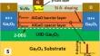
Fabrication and characterization of modulation-doped β-(AlxGa1−x)2O3/Ga2O3 tri-metal FET utilizing ultra-high vacuum deposition based on plasma-assisted molecular beam epitaxy
This study investigates the design of MOD-FETs (modulation-doped field effect transistors) using β-Ga2O3 as the substrate material. The main focus is on understanding the impact of self-heating on the alteration of mobility of electrons profile. This paper introduces a model that takes into account the influence on temperature and doping on the electron mobility in β-Ga2O3. Furthermore, it offers estimations for the conductivity of heat of β-Ga2O3, considering the influence of temperature and crystalline orientation. Furthermore, we showcase a practical example of modulation-doped β-(AlxGa1-x)2O3/Ga2O3 using a tri-metal FET where the energy level difference between the conduction bands and the presence of undesired channels in the barrier layer determines the maximum sheet carrier density in this structure. These channels enable the transfer of electrons from both the bottom and upper portions of the β-Ga2O3 quantum well. Using modulation doping, the proposed structure exhibited an ultimate current drain of 250 mA/m, a peak conductivity of 40 ms/m, and a potential of 10.0 V at ambient temperature. The electrical characteristics of the TMG device were evaluated by comparing it to the double-metal gate (DMG) device using the Atlas Silvaco TCAD simulation for analysis of performance. The results indicate that, the suggested device exhibits greater efficiency in terms of conductivity, current gain cut-off frequency, and energy gain cut-off frequency as compared to DMG transistors. The measured electric field in this example is a consequence of using a Tri-Metal Gate architecture (TMG) to regulate the channel. The designed setup achieves peak frequency of 45.5/50.5 gigahertz with a gate length of 0.2 mm. This discovery highlights the potential of using the β-(AlxGa1−x)2O3/Ga2O3 with tri-metal FET architecture as a promising method for high-power radio frequency operations.
期刊介绍:
The Journal of Materials Science: Materials in Electronics is an established refereed companion to the Journal of Materials Science. It publishes papers on materials and their applications in modern electronics, covering the ground between fundamental science, such as semiconductor physics, and work concerned specifically with applications. It explores the growth and preparation of new materials, as well as their processing, fabrication, bonding and encapsulation, together with the reliability, failure analysis, quality assurance and characterization related to the whole range of applications in electronics. The Journal presents papers in newly developing fields such as low dimensional structures and devices, optoelectronics including III-V compounds, glasses and linear/non-linear crystal materials and lasers, high Tc superconductors, conducting polymers, thick film materials and new contact technologies, as well as the established electronics device and circuit materials.

 求助内容:
求助内容: 应助结果提醒方式:


