Jinping Zhang, Mengxiao Li, Yunxiang Huang, Bing Xiao, Bo Zhang
{"title":"具有窄网格和浮动 P 区的双注入增强型超级结 TIGBT","authors":"Jinping Zhang, Mengxiao Li, Yunxiang Huang, Bing Xiao, Bo Zhang","doi":"10.1007/s10825-024-02218-w","DOIUrl":null,"url":null,"abstract":"<div><p>For the conventional super junction trench insulated gate bipolar transistor (SJ-TIGBT), the higher the N/P column doping concentration (<i>N</i><sub>c</sub>), the better the electrical characteristics can be obtained. However, considering the negative impact of charge imbalance of the N/P column on the breakdown voltage (<i>BV</i>), the value of <i>N</i><sub>c</sub> is limited, which limits the improvement of device performances. In this paper, a novel SJ-TIGBT with narrow mesa (NM) and floating-P (FP) region (NMFP-SJ-TIGBT) is proposed. The electrical characteristics of the proposed SJ-TIGBT are significantly enhanced owing to the dual injection enhancement effect provided by the NM and FP region. Moreover, for the proposed SJ device, the excellent performance obtained in the lower <i>N</i><sub>c</sub> regime alleviates the negative impact of charge imbalance of N/P column on the <i>BV</i>, which greatly improves its fabrication process tolerance. The simulation results show that compared to the conventional SJ-TIGBT (SJ-TIGBT-A), a SJ-TIGBT with an n-injector layer (SJ-TIGBT-B) and a SJ-TIGBT with a floating-P column under the gate (SJ-TIGBT-C), the proposed structure demonstrates a significantly lower and almost constant on-state voltage drop (<i>V</i><sub>ceon</sub>). At a collector current density of 100 A/cm<sup>2</sup> and <i>N</i><sub>c</sub> of 1 × 10<sup>15</sup> cm<sup>−3</sup>, the <i>V</i><sub>ceon</sub> of the proposed SJ-TIGBT is 74.9%, 41.1% and 26.1% lower than that of the SJ-TIGBT-A, SJ-TIGBT-B and SJ-TIGBT-C, respectively. With the same <i>V</i><sub>ceon</sub> of 1.05 V and <i>N</i><sub>c</sub> of 1 × 10<sup>15</sup> cm<sup>−3</sup>, the turn-off loss of the proposed SJ-TIGBT is only 6.44 mJ/cm<sup>2</sup>, which is 73.7% and 35.4% lower than that of SJ-TIGBT-B and SJ-TIGBT-C, respectively.</p></div>","PeriodicalId":620,"journal":{"name":"Journal of Computational Electronics","volume":"23 6","pages":"1345 - 1354"},"PeriodicalIF":2.2000,"publicationDate":"2024-08-23","publicationTypes":"Journal Article","fieldsOfStudy":null,"isOpenAccess":false,"openAccessPdf":"","citationCount":"0","resultStr":"{\"title\":\"Dual injection enhanced super junction TIGBT with narrow mesa and floating-P region\",\"authors\":\"Jinping Zhang, Mengxiao Li, Yunxiang Huang, Bing Xiao, Bo Zhang\",\"doi\":\"10.1007/s10825-024-02218-w\",\"DOIUrl\":null,\"url\":null,\"abstract\":\"<div><p>For the conventional super junction trench insulated gate bipolar transistor (SJ-TIGBT), the higher the N/P column doping concentration (<i>N</i><sub>c</sub>), the better the electrical characteristics can be obtained. However, considering the negative impact of charge imbalance of the N/P column on the breakdown voltage (<i>BV</i>), the value of <i>N</i><sub>c</sub> is limited, which limits the improvement of device performances. In this paper, a novel SJ-TIGBT with narrow mesa (NM) and floating-P (FP) region (NMFP-SJ-TIGBT) is proposed. The electrical characteristics of the proposed SJ-TIGBT are significantly enhanced owing to the dual injection enhancement effect provided by the NM and FP region. Moreover, for the proposed SJ device, the excellent performance obtained in the lower <i>N</i><sub>c</sub> regime alleviates the negative impact of charge imbalance of N/P column on the <i>BV</i>, which greatly improves its fabrication process tolerance. The simulation results show that compared to the conventional SJ-TIGBT (SJ-TIGBT-A), a SJ-TIGBT with an n-injector layer (SJ-TIGBT-B) and a SJ-TIGBT with a floating-P column under the gate (SJ-TIGBT-C), the proposed structure demonstrates a significantly lower and almost constant on-state voltage drop (<i>V</i><sub>ceon</sub>). At a collector current density of 100 A/cm<sup>2</sup> and <i>N</i><sub>c</sub> of 1 × 10<sup>15</sup> cm<sup>−3</sup>, the <i>V</i><sub>ceon</sub> of the proposed SJ-TIGBT is 74.9%, 41.1% and 26.1% lower than that of the SJ-TIGBT-A, SJ-TIGBT-B and SJ-TIGBT-C, respectively. With the same <i>V</i><sub>ceon</sub> of 1.05 V and <i>N</i><sub>c</sub> of 1 × 10<sup>15</sup> cm<sup>−3</sup>, the turn-off loss of the proposed SJ-TIGBT is only 6.44 mJ/cm<sup>2</sup>, which is 73.7% and 35.4% lower than that of SJ-TIGBT-B and SJ-TIGBT-C, respectively.</p></div>\",\"PeriodicalId\":620,\"journal\":{\"name\":\"Journal of Computational Electronics\",\"volume\":\"23 6\",\"pages\":\"1345 - 1354\"},\"PeriodicalIF\":2.2000,\"publicationDate\":\"2024-08-23\",\"publicationTypes\":\"Journal Article\",\"fieldsOfStudy\":null,\"isOpenAccess\":false,\"openAccessPdf\":\"\",\"citationCount\":\"0\",\"resultStr\":null,\"platform\":\"Semanticscholar\",\"paperid\":null,\"PeriodicalName\":\"Journal of Computational Electronics\",\"FirstCategoryId\":\"5\",\"ListUrlMain\":\"https://link.springer.com/article/10.1007/s10825-024-02218-w\",\"RegionNum\":4,\"RegionCategory\":\"工程技术\",\"ArticlePicture\":[],\"TitleCN\":null,\"AbstractTextCN\":null,\"PMCID\":null,\"EPubDate\":\"\",\"PubModel\":\"\",\"JCR\":\"Q3\",\"JCRName\":\"ENGINEERING, ELECTRICAL & ELECTRONIC\",\"Score\":null,\"Total\":0}","platform":"Semanticscholar","paperid":null,"PeriodicalName":"Journal of Computational Electronics","FirstCategoryId":"5","ListUrlMain":"https://link.springer.com/article/10.1007/s10825-024-02218-w","RegionNum":4,"RegionCategory":"工程技术","ArticlePicture":[],"TitleCN":null,"AbstractTextCN":null,"PMCID":null,"EPubDate":"","PubModel":"","JCR":"Q3","JCRName":"ENGINEERING, ELECTRICAL & ELECTRONIC","Score":null,"Total":0}
Dual injection enhanced super junction TIGBT with narrow mesa and floating-P region
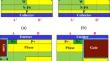
For the conventional super junction trench insulated gate bipolar transistor (SJ-TIGBT), the higher the N/P column doping concentration (Nc), the better the electrical characteristics can be obtained. However, considering the negative impact of charge imbalance of the N/P column on the breakdown voltage (BV), the value of Nc is limited, which limits the improvement of device performances. In this paper, a novel SJ-TIGBT with narrow mesa (NM) and floating-P (FP) region (NMFP-SJ-TIGBT) is proposed. The electrical characteristics of the proposed SJ-TIGBT are significantly enhanced owing to the dual injection enhancement effect provided by the NM and FP region. Moreover, for the proposed SJ device, the excellent performance obtained in the lower Nc regime alleviates the negative impact of charge imbalance of N/P column on the BV, which greatly improves its fabrication process tolerance. The simulation results show that compared to the conventional SJ-TIGBT (SJ-TIGBT-A), a SJ-TIGBT with an n-injector layer (SJ-TIGBT-B) and a SJ-TIGBT with a floating-P column under the gate (SJ-TIGBT-C), the proposed structure demonstrates a significantly lower and almost constant on-state voltage drop (Vceon). At a collector current density of 100 A/cm2 and Nc of 1 × 1015 cm−3, the Vceon of the proposed SJ-TIGBT is 74.9%, 41.1% and 26.1% lower than that of the SJ-TIGBT-A, SJ-TIGBT-B and SJ-TIGBT-C, respectively. With the same Vceon of 1.05 V and Nc of 1 × 1015 cm−3, the turn-off loss of the proposed SJ-TIGBT is only 6.44 mJ/cm2, which is 73.7% and 35.4% lower than that of SJ-TIGBT-B and SJ-TIGBT-C, respectively.
期刊介绍:
he Journal of Computational Electronics brings together research on all aspects of modeling and simulation of modern electronics. This includes optical, electronic, mechanical, and quantum mechanical aspects, as well as research on the underlying mathematical algorithms and computational details. The related areas of energy conversion/storage and of molecular and biological systems, in which the thrust is on the charge transport, electronic, mechanical, and optical properties, are also covered.
In particular, we encourage manuscripts dealing with device simulation; with optical and optoelectronic systems and photonics; with energy storage (e.g. batteries, fuel cells) and harvesting (e.g. photovoltaic), with simulation of circuits, VLSI layout, logic and architecture (based on, for example, CMOS devices, quantum-cellular automata, QBITs, or single-electron transistors); with electromagnetic simulations (such as microwave electronics and components); or with molecular and biological systems. However, in all these cases, the submitted manuscripts should explicitly address the electronic properties of the relevant systems, materials, or devices and/or present novel contributions to the physical models, computational strategies, or numerical algorithms.

 求助内容:
求助内容: 应助结果提醒方式:


