{"title":"带 Si3N4-SiO2 叠层栅极的 MOSFET 中总电离剂量和单次栅极破裂的协同效应","authors":"Rongxing Cao, Hanxun Liu, Kejia Wang, Dike Hu, Yiyuan Wang, Xianghua Zeng, Yuxiong Xue","doi":"10.1007/s10825-024-02227-9","DOIUrl":null,"url":null,"abstract":"<div><p>The synergistic effect of total ionizing dose on single event gate rupture (SEGR) was simulated in the vertical double diffusion metal oxide semiconductor device with SiO<sub>2</sub>–Si<sub>3</sub>N<sub>4</sub> stacked gate layer. In comparison to the device with a single SiO<sub>2</sub> gate layer, the synergistic effect was revealed to be suppressed in the device with SiO<sub>2</sub>–Si<sub>3</sub>N<sub>4</sub> stacked layer. The mechanism is that the oxide layer is a sensitive area of the SEGR effect. Compared with the single SiO<sub>2</sub> layer, the superposition of the additional electric field formed by the trapped holes in the sensitive area of the stacked layer leads to a decrease in the sensitivity of the synergistic effect, which is more obvious with increasing the volume of the Si<sub>3</sub>N<sub>4</sub> layer.</p></div>","PeriodicalId":620,"journal":{"name":"Journal of Computational Electronics","volume":"23 6","pages":"1298 - 1305"},"PeriodicalIF":2.2000,"publicationDate":"2024-09-06","publicationTypes":"Journal Article","fieldsOfStudy":null,"isOpenAccess":false,"openAccessPdf":"","citationCount":"0","resultStr":"{\"title\":\"Synergistic effect of total ionizing dose and single event gate rupture in MOSFET with Si3N4–SiO2 stacked gate\",\"authors\":\"Rongxing Cao, Hanxun Liu, Kejia Wang, Dike Hu, Yiyuan Wang, Xianghua Zeng, Yuxiong Xue\",\"doi\":\"10.1007/s10825-024-02227-9\",\"DOIUrl\":null,\"url\":null,\"abstract\":\"<div><p>The synergistic effect of total ionizing dose on single event gate rupture (SEGR) was simulated in the vertical double diffusion metal oxide semiconductor device with SiO<sub>2</sub>–Si<sub>3</sub>N<sub>4</sub> stacked gate layer. In comparison to the device with a single SiO<sub>2</sub> gate layer, the synergistic effect was revealed to be suppressed in the device with SiO<sub>2</sub>–Si<sub>3</sub>N<sub>4</sub> stacked layer. The mechanism is that the oxide layer is a sensitive area of the SEGR effect. Compared with the single SiO<sub>2</sub> layer, the superposition of the additional electric field formed by the trapped holes in the sensitive area of the stacked layer leads to a decrease in the sensitivity of the synergistic effect, which is more obvious with increasing the volume of the Si<sub>3</sub>N<sub>4</sub> layer.</p></div>\",\"PeriodicalId\":620,\"journal\":{\"name\":\"Journal of Computational Electronics\",\"volume\":\"23 6\",\"pages\":\"1298 - 1305\"},\"PeriodicalIF\":2.2000,\"publicationDate\":\"2024-09-06\",\"publicationTypes\":\"Journal Article\",\"fieldsOfStudy\":null,\"isOpenAccess\":false,\"openAccessPdf\":\"\",\"citationCount\":\"0\",\"resultStr\":null,\"platform\":\"Semanticscholar\",\"paperid\":null,\"PeriodicalName\":\"Journal of Computational Electronics\",\"FirstCategoryId\":\"5\",\"ListUrlMain\":\"https://link.springer.com/article/10.1007/s10825-024-02227-9\",\"RegionNum\":4,\"RegionCategory\":\"工程技术\",\"ArticlePicture\":[],\"TitleCN\":null,\"AbstractTextCN\":null,\"PMCID\":null,\"EPubDate\":\"\",\"PubModel\":\"\",\"JCR\":\"Q3\",\"JCRName\":\"ENGINEERING, ELECTRICAL & ELECTRONIC\",\"Score\":null,\"Total\":0}","platform":"Semanticscholar","paperid":null,"PeriodicalName":"Journal of Computational Electronics","FirstCategoryId":"5","ListUrlMain":"https://link.springer.com/article/10.1007/s10825-024-02227-9","RegionNum":4,"RegionCategory":"工程技术","ArticlePicture":[],"TitleCN":null,"AbstractTextCN":null,"PMCID":null,"EPubDate":"","PubModel":"","JCR":"Q3","JCRName":"ENGINEERING, ELECTRICAL & ELECTRONIC","Score":null,"Total":0}
Synergistic effect of total ionizing dose and single event gate rupture in MOSFET with Si3N4–SiO2 stacked gate
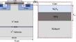
The synergistic effect of total ionizing dose on single event gate rupture (SEGR) was simulated in the vertical double diffusion metal oxide semiconductor device with SiO2–Si3N4 stacked gate layer. In comparison to the device with a single SiO2 gate layer, the synergistic effect was revealed to be suppressed in the device with SiO2–Si3N4 stacked layer. The mechanism is that the oxide layer is a sensitive area of the SEGR effect. Compared with the single SiO2 layer, the superposition of the additional electric field formed by the trapped holes in the sensitive area of the stacked layer leads to a decrease in the sensitivity of the synergistic effect, which is more obvious with increasing the volume of the Si3N4 layer.
期刊介绍:
he Journal of Computational Electronics brings together research on all aspects of modeling and simulation of modern electronics. This includes optical, electronic, mechanical, and quantum mechanical aspects, as well as research on the underlying mathematical algorithms and computational details. The related areas of energy conversion/storage and of molecular and biological systems, in which the thrust is on the charge transport, electronic, mechanical, and optical properties, are also covered.
In particular, we encourage manuscripts dealing with device simulation; with optical and optoelectronic systems and photonics; with energy storage (e.g. batteries, fuel cells) and harvesting (e.g. photovoltaic), with simulation of circuits, VLSI layout, logic and architecture (based on, for example, CMOS devices, quantum-cellular automata, QBITs, or single-electron transistors); with electromagnetic simulations (such as microwave electronics and components); or with molecular and biological systems. However, in all these cases, the submitted manuscripts should explicitly address the electronic properties of the relevant systems, materials, or devices and/or present novel contributions to the physical models, computational strategies, or numerical algorithms.

 求助内容:
求助内容: 应助结果提醒方式:


