在硅晶片上均匀大规模合成 GaAs/GaInNAs/GaAs 纳米线,用于在近红外区域工作的器件

IF 5.3 2区 材料科学 Q2 MATERIALS SCIENCE, MULTIDISCIPLINARY
Keisuke Minehisa, Kaito Nakama, Hidetoshi Hashimoto, Fumitaro Ishikawa
{"title":"在硅晶片上均匀大规模合成 GaAs/GaInNAs/GaAs 纳米线,用于在近红外区域工作的器件","authors":"Keisuke Minehisa, Kaito Nakama, Hidetoshi Hashimoto, Fumitaro Ishikawa","doi":"10.1021/acsanm.4c03855","DOIUrl":null,"url":null,"abstract":"The synthesis of semiconductor nanowires (NWs) with near-infrared light-absorbing and light-emission properties is presented. Gallium (Ga)-induced vapor–liquid–solid growth is used to produce GaAs/GaInNAs/GaAs core–multishell NWs on a 2 in. Si(111) wafer using plasma-assisted molecular beam epitaxy. The GaInNAs shell consists of 11% indium (In) and varying compositions of nitrogen (N) of up to 1.9%. The NWs serve as an antireflective material, showing that the entire substrate is black. Photoluminescence measurements at room temperature validate the expansion of the operating wavelength into the near-infrared region as the N content in the NWs increases. The GaInNAs sample with 11% In and 1.2% N shows homogeneous luminescence at 1100 nm across the entire 2 in. Si substrate. The reflectance of the NW samples is low, less than 2%, and the absorption edge can be controlled by modifying the composition of In and N indicating the potential application of large-scale photoelectric conversion, such as solar cells.","PeriodicalId":6,"journal":{"name":"ACS Applied Nano Materials","volume":null,"pages":null},"PeriodicalIF":5.3000,"publicationDate":"2024-09-13","publicationTypes":"Journal Article","fieldsOfStudy":null,"isOpenAccess":false,"openAccessPdf":"","citationCount":"0","resultStr":"{\"title\":\"Homogeneous Large-Scale Synthesis of GaAs/GaInNAs/GaAs Nanowires on a Si Wafer for Devices Operating in the Near-Infrared Region\",\"authors\":\"Keisuke Minehisa, Kaito Nakama, Hidetoshi Hashimoto, Fumitaro Ishikawa\",\"doi\":\"10.1021/acsanm.4c03855\",\"DOIUrl\":null,\"url\":null,\"abstract\":\"The synthesis of semiconductor nanowires (NWs) with near-infrared light-absorbing and light-emission properties is presented. Gallium (Ga)-induced vapor–liquid–solid growth is used to produce GaAs/GaInNAs/GaAs core–multishell NWs on a 2 in. Si(111) wafer using plasma-assisted molecular beam epitaxy. The GaInNAs shell consists of 11% indium (In) and varying compositions of nitrogen (N) of up to 1.9%. The NWs serve as an antireflective material, showing that the entire substrate is black. Photoluminescence measurements at room temperature validate the expansion of the operating wavelength into the near-infrared region as the N content in the NWs increases. The GaInNAs sample with 11% In and 1.2% N shows homogeneous luminescence at 1100 nm across the entire 2 in. Si substrate. The reflectance of the NW samples is low, less than 2%, and the absorption edge can be controlled by modifying the composition of In and N indicating the potential application of large-scale photoelectric conversion, such as solar cells.\",\"PeriodicalId\":6,\"journal\":{\"name\":\"ACS Applied Nano Materials\",\"volume\":null,\"pages\":null},\"PeriodicalIF\":5.3000,\"publicationDate\":\"2024-09-13\",\"publicationTypes\":\"Journal Article\",\"fieldsOfStudy\":null,\"isOpenAccess\":false,\"openAccessPdf\":\"\",\"citationCount\":\"0\",\"resultStr\":null,\"platform\":\"Semanticscholar\",\"paperid\":null,\"PeriodicalName\":\"ACS Applied Nano Materials\",\"FirstCategoryId\":\"88\",\"ListUrlMain\":\"https://doi.org/10.1021/acsanm.4c03855\",\"RegionNum\":2,\"RegionCategory\":\"材料科学\",\"ArticlePicture\":[],\"TitleCN\":null,\"AbstractTextCN\":null,\"PMCID\":null,\"EPubDate\":\"\",\"PubModel\":\"\",\"JCR\":\"Q2\",\"JCRName\":\"MATERIALS SCIENCE, MULTIDISCIPLINARY\",\"Score\":null,\"Total\":0}","platform":"Semanticscholar","paperid":null,"PeriodicalName":"ACS Applied Nano Materials","FirstCategoryId":"88","ListUrlMain":"https://doi.org/10.1021/acsanm.4c03855","RegionNum":2,"RegionCategory":"材料科学","ArticlePicture":[],"TitleCN":null,"AbstractTextCN":null,"PMCID":null,"EPubDate":"","PubModel":"","JCR":"Q2","JCRName":"MATERIALS SCIENCE, MULTIDISCIPLINARY","Score":null,"Total":0}
引用次数: 0

摘要

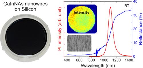
本文介绍了具有近红外光吸收和发射特性的半导体纳米线(NWs)的合成。利用等离子体辅助分子束外延技术,在一个 2 英寸的 Si(111) 晶圆上,通过镓(Ga)诱导的气-液-固生长,制备出 GaAs/GaInNAs/GaAs 核-多壳纳米线。GaInNAs 外壳由 11% 的铟(In)和不同成分的氮(N)(最高达 1.9%)组成。氮化铟镓作为一种抗反射材料,使整个基底呈黑色。室温下的光致发光测量证实,随着氮化物中氮含量的增加,工作波长扩展到了近红外区域。含 11% In 和 1.2% N 的 GaInNAs 样品在整个 2 英寸硅衬底上显示出 1100 nm 的均匀发光。NW 样品的反射率很低,小于 2%,而且可以通过改变 In 和 N 的成分来控制吸收边缘,这表明其具有大规模光电转换(如太阳能电池)的应用潜力。
本文章由计算机程序翻译,如有差异,请以英文原文为准。

Homogeneous Large-Scale Synthesis of GaAs/GaInNAs/GaAs Nanowires on a Si Wafer for Devices Operating in the Near-Infrared Region

Homogeneous Large-Scale Synthesis of GaAs/GaInNAs/GaAs Nanowires on a Si Wafer for Devices Operating in the Near-Infrared Region
The synthesis of semiconductor nanowires (NWs) with near-infrared light-absorbing and light-emission properties is presented. Gallium (Ga)-induced vapor–liquid–solid growth is used to produce GaAs/GaInNAs/GaAs core–multishell NWs on a 2 in. Si(111) wafer using plasma-assisted molecular beam epitaxy. The GaInNAs shell consists of 11% indium (In) and varying compositions of nitrogen (N) of up to 1.9%. The NWs serve as an antireflective material, showing that the entire substrate is black. Photoluminescence measurements at room temperature validate the expansion of the operating wavelength into the near-infrared region as the N content in the NWs increases. The GaInNAs sample with 11% In and 1.2% N shows homogeneous luminescence at 1100 nm across the entire 2 in. Si substrate. The reflectance of the NW samples is low, less than 2%, and the absorption edge can be controlled by modifying the composition of In and N indicating the potential application of large-scale photoelectric conversion, such as solar cells.
求助全文
通过发布文献求助,成功后即可免费获取论文全文。 去求助
来源期刊
CiteScore
8.30
自引率
3.40%
发文量
1601
期刊介绍: ACS Applied Nano Materials is an interdisciplinary journal publishing original research covering all aspects of engineering, chemistry, physics and biology relevant to applications of nanomaterials. The journal is devoted to reports of new and original experimental and theoretical research of an applied nature that integrate knowledge in the areas of materials, engineering, physics, bioscience, and chemistry into important applications of nanomaterials.
×
引用
GB/T 7714-2015
复制
MLA
复制
APA
复制
导出至
BibTeX EndNote RefMan NoteFirst NoteExpress
×
提示
您的信息不完整,为了账户安全,请先补充。
现在去补充
×
提示
您因"违规操作"
具体请查看互助需知
我知道了
×
提示
确定
请完成安全验证×
copy
已复制链接
快去分享给好友吧!
我知道了
右上角分享
点击右上角分享
0
联系我们:info@booksci.cn Book学术提供免费学术资源搜索服务,方便国内外学者检索中英文文献。致力于提供最便捷和优质的服务体验。 Copyright © 2023 布克学术 All rights reserved.
京ICP备2023020795号-1
ghs 京公网安备 11010802042870号
Book学术文献互助
Book学术文献互助群
群 号:481959085
Book学术官方微信