Matteo Gardella, Giorgio Zambito, Giulio Ferrando, Francesco Bisio, Maria Caterina Giordano and Francesco Buatier de Mongeot
{"title":"用于可见光能量转换的大面积范德华 MoS2-WS2 异质结构†。","authors":"Matteo Gardella, Giorgio Zambito, Giulio Ferrando, Francesco Bisio, Maria Caterina Giordano and Francesco Buatier de Mongeot","doi":"10.1039/D3LF00220A","DOIUrl":null,"url":null,"abstract":"<p >In recent years, high-quality transition metal dichalcogenide layers and their van der Waals heterostructures, based on either mechanical exfoliation or chemical vapor deposition, have been successfully employed for the fabrication of electronic and optoelectronic devices, demonstrating their potential towards the integration or replacement of traditional semiconductor technologies. However, these fabrication techniques rely on single flakes with limited size on the scale of tens of micrometers. Here, we propose a large-scale growth process based on physical deposition that enables uniform coverage over cm<small><sup>2</sup></small> areas. This method allows us to fabricate a large area prototype van der Waals heterostructure by vertically stacking in sequence few-layer WS<small><sub>2</sub></small>–MoS<small><sub>2</sub></small> films, forming a type-II heterojunction which shows enhanced photocatalytic dissociation efficiency compared to a reference MoS<small><sub>2</sub></small> film. Upon addition of a bottom graphene transparent electrode and a top Au contact, under illumination conditions we find evidence of photovoltage and photocurrent generation, thus demonstrating the potential of our large-scale 2D-TMD growth process in view of scalable, self-powered photoconversion applications.</p>","PeriodicalId":101138,"journal":{"name":"RSC Applied Interfaces","volume":" 5","pages":" 1001-1011"},"PeriodicalIF":0.0000,"publicationDate":"2024-04-27","publicationTypes":"Journal Article","fieldsOfStudy":null,"isOpenAccess":false,"openAccessPdf":"https://pubs.rsc.org/en/content/articlepdf/2024/lf/d3lf00220a?page=search","citationCount":"0","resultStr":"{\"title\":\"Large area van der Waals MoS2–WS2 heterostructures for visible-light energy conversion†\",\"authors\":\"Matteo Gardella, Giorgio Zambito, Giulio Ferrando, Francesco Bisio, Maria Caterina Giordano and Francesco Buatier de Mongeot\",\"doi\":\"10.1039/D3LF00220A\",\"DOIUrl\":null,\"url\":null,\"abstract\":\"<p >In recent years, high-quality transition metal dichalcogenide layers and their van der Waals heterostructures, based on either mechanical exfoliation or chemical vapor deposition, have been successfully employed for the fabrication of electronic and optoelectronic devices, demonstrating their potential towards the integration or replacement of traditional semiconductor technologies. However, these fabrication techniques rely on single flakes with limited size on the scale of tens of micrometers. Here, we propose a large-scale growth process based on physical deposition that enables uniform coverage over cm<small><sup>2</sup></small> areas. This method allows us to fabricate a large area prototype van der Waals heterostructure by vertically stacking in sequence few-layer WS<small><sub>2</sub></small>–MoS<small><sub>2</sub></small> films, forming a type-II heterojunction which shows enhanced photocatalytic dissociation efficiency compared to a reference MoS<small><sub>2</sub></small> film. Upon addition of a bottom graphene transparent electrode and a top Au contact, under illumination conditions we find evidence of photovoltage and photocurrent generation, thus demonstrating the potential of our large-scale 2D-TMD growth process in view of scalable, self-powered photoconversion applications.</p>\",\"PeriodicalId\":101138,\"journal\":{\"name\":\"RSC Applied Interfaces\",\"volume\":\" 5\",\"pages\":\" 1001-1011\"},\"PeriodicalIF\":0.0000,\"publicationDate\":\"2024-04-27\",\"publicationTypes\":\"Journal Article\",\"fieldsOfStudy\":null,\"isOpenAccess\":false,\"openAccessPdf\":\"https://pubs.rsc.org/en/content/articlepdf/2024/lf/d3lf00220a?page=search\",\"citationCount\":\"0\",\"resultStr\":null,\"platform\":\"Semanticscholar\",\"paperid\":null,\"PeriodicalName\":\"RSC Applied Interfaces\",\"FirstCategoryId\":\"1085\",\"ListUrlMain\":\"https://pubs.rsc.org/en/content/articlelanding/2024/lf/d3lf00220a\",\"RegionNum\":0,\"RegionCategory\":null,\"ArticlePicture\":[],\"TitleCN\":null,\"AbstractTextCN\":null,\"PMCID\":null,\"EPubDate\":\"\",\"PubModel\":\"\",\"JCR\":\"\",\"JCRName\":\"\",\"Score\":null,\"Total\":0}","platform":"Semanticscholar","paperid":null,"PeriodicalName":"RSC Applied Interfaces","FirstCategoryId":"1085","ListUrlMain":"https://pubs.rsc.org/en/content/articlelanding/2024/lf/d3lf00220a","RegionNum":0,"RegionCategory":null,"ArticlePicture":[],"TitleCN":null,"AbstractTextCN":null,"PMCID":null,"EPubDate":"","PubModel":"","JCR":"","JCRName":"","Score":null,"Total":0}
引用次数: 0
摘要
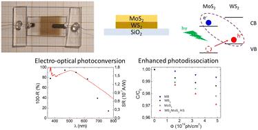
近年来,基于机械剥离或化学气相沉积的高质量过渡金属二卤化物层及其范德华异质结构已被成功用于制造电子和光电设备,显示了其集成或替代传统半导体技术的潜力。然而,这些制造技术依赖于尺寸有限的数十微米级单片。在这里,我们提出了一种基于物理沉积的大规模生长工艺,它能在平方厘米的区域内实现均匀覆盖。通过这种方法,我们可以依次垂直堆叠几层 WS2-MoS2 薄膜,制造出大面积的范德华异质结构原型,形成 II 型异质结,与参考 MoS2 薄膜相比,这种异质结显示出更高的光催化解离效率。在加入底部石墨烯透明电极和顶部金触点后,我们发现在照明条件下会产生光电压和光电流,从而证明了我们的大规模二维-TMD 生长工艺在可扩展的自供电光电转换应用方面的潜力。
Large area van der Waals MoS2–WS2 heterostructures for visible-light energy conversion†
In recent years, high-quality transition metal dichalcogenide layers and their van der Waals heterostructures, based on either mechanical exfoliation or chemical vapor deposition, have been successfully employed for the fabrication of electronic and optoelectronic devices, demonstrating their potential towards the integration or replacement of traditional semiconductor technologies. However, these fabrication techniques rely on single flakes with limited size on the scale of tens of micrometers. Here, we propose a large-scale growth process based on physical deposition that enables uniform coverage over cm2 areas. This method allows us to fabricate a large area prototype van der Waals heterostructure by vertically stacking in sequence few-layer WS2–MoS2 films, forming a type-II heterojunction which shows enhanced photocatalytic dissociation efficiency compared to a reference MoS2 film. Upon addition of a bottom graphene transparent electrode and a top Au contact, under illumination conditions we find evidence of photovoltage and photocurrent generation, thus demonstrating the potential of our large-scale 2D-TMD growth process in view of scalable, self-powered photoconversion applications.

 求助内容:
求助内容: 应助结果提醒方式:


