N. D. Il'inskaya, S. A. Karandashev, T. S. Lukhmyrina, B. A. Matveev, M. A. Remennyi and A. E. Chernyakov
{"title":"金属/n-InAs 结构中的电流诱导冷却","authors":"N. D. Il'inskaya, S. A. Karandashev, T. S. Lukhmyrina, B. A. Matveev, M. A. Remennyi and A. E. Chernyakov","doi":"10.1039/D4LF00032C","DOIUrl":null,"url":null,"abstract":"<p >This paper focuses on the specific features of an Ohmic contact on undoped <em>n</em>-InAs (<em>n</em> = 2 × 10<small><sup>16</sup></small> cm<small><sup>−3</sup></small>) that could be used for temperature stabilization and/or temperature reduction in electronic devices, mainly operating in the 3–5 μm mid-IR range. This feature has been demonstrated in a 100 μm thick <em>n</em>-InAs slab with three unannealed Cr–Au–Ni–Au contacts formed <em>via</em> evaporation in vacuum. The <em>I</em>–<em>V</em> characteristics showed no deviation from Ohm's law in the temperature range 77–340 K, manifesting a contact resistance ranging from 3.6 × 10<small><sup>−5</sup></small> to 7.2 × 10<small><sup>−5</sup></small> Ω cm<small><sup>2</sup></small> at room temperature. The 2D thermal radiation distribution and the temperature distribution over the <em>n</em>-InAs surface opposite the contact side surface was obtained <em>via</em> a pre-calibrated IR microscope operating at a wavelength of 3 μm. The measurements revealed a current dependent temperature decline in the area adjacent to the negatively biased contact: at the applied power of 5 mW, cooling as strong as Δ<em>T</em> ≈ 1 K occurred at an ambient temperature of 340 K. The results show potential for the fabrication of heterostructures with a “built-in” cooler that is monolithically integrated with another electronic device.</p>","PeriodicalId":101138,"journal":{"name":"RSC Applied Interfaces","volume":" 5","pages":" 1031-1035"},"PeriodicalIF":0.0000,"publicationDate":"2024-04-30","publicationTypes":"Journal Article","fieldsOfStudy":null,"isOpenAccess":false,"openAccessPdf":"https://pubs.rsc.org/en/content/articlepdf/2024/lf/d4lf00032c?page=search","citationCount":"0","resultStr":"{\"title\":\"Current induced cooling in a metal/n-InAs structure\",\"authors\":\"N. D. Il'inskaya, S. A. Karandashev, T. S. Lukhmyrina, B. A. Matveev, M. A. Remennyi and A. E. Chernyakov\",\"doi\":\"10.1039/D4LF00032C\",\"DOIUrl\":null,\"url\":null,\"abstract\":\"<p >This paper focuses on the specific features of an Ohmic contact on undoped <em>n</em>-InAs (<em>n</em> = 2 × 10<small><sup>16</sup></small> cm<small><sup>−3</sup></small>) that could be used for temperature stabilization and/or temperature reduction in electronic devices, mainly operating in the 3–5 μm mid-IR range. This feature has been demonstrated in a 100 μm thick <em>n</em>-InAs slab with three unannealed Cr–Au–Ni–Au contacts formed <em>via</em> evaporation in vacuum. The <em>I</em>–<em>V</em> characteristics showed no deviation from Ohm's law in the temperature range 77–340 K, manifesting a contact resistance ranging from 3.6 × 10<small><sup>−5</sup></small> to 7.2 × 10<small><sup>−5</sup></small> Ω cm<small><sup>2</sup></small> at room temperature. The 2D thermal radiation distribution and the temperature distribution over the <em>n</em>-InAs surface opposite the contact side surface was obtained <em>via</em> a pre-calibrated IR microscope operating at a wavelength of 3 μm. The measurements revealed a current dependent temperature decline in the area adjacent to the negatively biased contact: at the applied power of 5 mW, cooling as strong as Δ<em>T</em> ≈ 1 K occurred at an ambient temperature of 340 K. The results show potential for the fabrication of heterostructures with a “built-in” cooler that is monolithically integrated with another electronic device.</p>\",\"PeriodicalId\":101138,\"journal\":{\"name\":\"RSC Applied Interfaces\",\"volume\":\" 5\",\"pages\":\" 1031-1035\"},\"PeriodicalIF\":0.0000,\"publicationDate\":\"2024-04-30\",\"publicationTypes\":\"Journal Article\",\"fieldsOfStudy\":null,\"isOpenAccess\":false,\"openAccessPdf\":\"https://pubs.rsc.org/en/content/articlepdf/2024/lf/d4lf00032c?page=search\",\"citationCount\":\"0\",\"resultStr\":null,\"platform\":\"Semanticscholar\",\"paperid\":null,\"PeriodicalName\":\"RSC Applied Interfaces\",\"FirstCategoryId\":\"1085\",\"ListUrlMain\":\"https://pubs.rsc.org/en/content/articlelanding/2024/lf/d4lf00032c\",\"RegionNum\":0,\"RegionCategory\":null,\"ArticlePicture\":[],\"TitleCN\":null,\"AbstractTextCN\":null,\"PMCID\":null,\"EPubDate\":\"\",\"PubModel\":\"\",\"JCR\":\"\",\"JCRName\":\"\",\"Score\":null,\"Total\":0}","platform":"Semanticscholar","paperid":null,"PeriodicalName":"RSC Applied Interfaces","FirstCategoryId":"1085","ListUrlMain":"https://pubs.rsc.org/en/content/articlelanding/2024/lf/d4lf00032c","RegionNum":0,"RegionCategory":null,"ArticlePicture":[],"TitleCN":null,"AbstractTextCN":null,"PMCID":null,"EPubDate":"","PubModel":"","JCR":"","JCRName":"","Score":null,"Total":0}
Current induced cooling in a metal/n-InAs structure
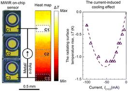
This paper focuses on the specific features of an Ohmic contact on undoped n-InAs (n = 2 × 1016 cm−3) that could be used for temperature stabilization and/or temperature reduction in electronic devices, mainly operating in the 3–5 μm mid-IR range. This feature has been demonstrated in a 100 μm thick n-InAs slab with three unannealed Cr–Au–Ni–Au contacts formed via evaporation in vacuum. The I–V characteristics showed no deviation from Ohm's law in the temperature range 77–340 K, manifesting a contact resistance ranging from 3.6 × 10⁻⁵ to 7.2 × 10⁻⁵ Ω cm2 at room temperature. The 2D thermal radiation distribution and the temperature distribution over the n-InAs surface opposite the contact side surface was obtained via a pre-calibrated IR microscope operating at a wavelength of 3 μm. The measurements revealed a current dependent temperature decline in the area adjacent to the negatively biased contact: at the applied power of 5 mW, cooling as strong as ΔT ≈ 1 K occurred at an ambient temperature of 340 K. The results show potential for the fabrication of heterostructures with a “built-in” cooler that is monolithically integrated with another electronic device.

 求助内容:
求助内容: 应助结果提醒方式:


