用于增强集成式 1 × 4 硅光子功率分配器的反向设计锥形配置

IF 6.5 2区 物理与天体物理 Q1 MATERIALS SCIENCE, MULTIDISCIPLINARY
Seokjin Hong, Jinhyeong Yoon, Junhyeong Kim, Berkay Neseli, Jae-Yong Kim, Hyo-Hoon Park, Hamza Kurt
{"title":"用于增强集成式 1 × 4 硅光子功率分配器的反向设计锥形配置","authors":"Seokjin Hong, Jinhyeong Yoon, Junhyeong Kim, Berkay Neseli, Jae-Yong Kim, Hyo-Hoon Park, Hamza Kurt","doi":"10.1515/nanoph-2024-0295","DOIUrl":null,"url":null,"abstract":"Once light is coupled to a photonic chip, its efficient distribution in terms of power splitting throughout silicon photonic circuits is very crucial. We present two types of 1 × 4 power splitters with different splitting ratios of 1:1:1:1 and 2:1:1:2. Various taper configurations were compared and analyzed to find the suitable configuration for the power splitter, and among them, parabolic tapers were chosen. The design parameters of the power splitter were determined by means of solving inverse design problems via incorporating particle swarm optimization that allows for overcoming the limitation of the intuition-based brute-force approach. The front and rear portions of the power splitters were optimized sequentially to alleviate local minima issues. The proposed power splitters have a compact footprint of 12.32 × 5 μm<jats:sup>2</jats:sup> and can be fabricated through a CMOS-compatible fabrication process. Two-stage power splitter trees were measured to enhance reliability in an experiment. As a result, the power splitter with a splitting ratio of 1:1:1:1 exhibited an experimentally measured insertion loss below 0.61 dB and an imbalance below 1.01 dB within the bandwidth of 1,518–1,565 nm. Also, the power splitter with a splitting ratio of 2:1:1:2 showed an insertion loss below 0.52 dB and a targeted imbalance below 1.15 dB within the bandwidth of 1,526–1,570 nm. Such inverse-designed power splitters can be an essential part of many large-scale photonic circuits including optical phased arrays, programmable photonics, and photonic computing chips.","PeriodicalId":19027,"journal":{"name":"Nanophotonics","volume":"4 1","pages":""},"PeriodicalIF":6.5000,"publicationDate":"2024-09-09","publicationTypes":"Journal Article","fieldsOfStudy":null,"isOpenAccess":false,"openAccessPdf":"","citationCount":"0","resultStr":"{\"title\":\"Inverse-designed taper configuration for the enhancement of integrated 1 × 4 silicon photonic power splitters\",\"authors\":\"Seokjin Hong, Jinhyeong Yoon, Junhyeong Kim, Berkay Neseli, Jae-Yong Kim, Hyo-Hoon Park, Hamza Kurt\",\"doi\":\"10.1515/nanoph-2024-0295\",\"DOIUrl\":null,\"url\":null,\"abstract\":\"Once light is coupled to a photonic chip, its efficient distribution in terms of power splitting throughout silicon photonic circuits is very crucial. We present two types of 1 × 4 power splitters with different splitting ratios of 1:1:1:1 and 2:1:1:2. Various taper configurations were compared and analyzed to find the suitable configuration for the power splitter, and among them, parabolic tapers were chosen. The design parameters of the power splitter were determined by means of solving inverse design problems via incorporating particle swarm optimization that allows for overcoming the limitation of the intuition-based brute-force approach. The front and rear portions of the power splitters were optimized sequentially to alleviate local minima issues. The proposed power splitters have a compact footprint of 12.32 × 5 μm<jats:sup>2</jats:sup> and can be fabricated through a CMOS-compatible fabrication process. Two-stage power splitter trees were measured to enhance reliability in an experiment. As a result, the power splitter with a splitting ratio of 1:1:1:1 exhibited an experimentally measured insertion loss below 0.61 dB and an imbalance below 1.01 dB within the bandwidth of 1,518–1,565 nm. Also, the power splitter with a splitting ratio of 2:1:1:2 showed an insertion loss below 0.52 dB and a targeted imbalance below 1.15 dB within the bandwidth of 1,526–1,570 nm. Such inverse-designed power splitters can be an essential part of many large-scale photonic circuits including optical phased arrays, programmable photonics, and photonic computing chips.\",\"PeriodicalId\":19027,\"journal\":{\"name\":\"Nanophotonics\",\"volume\":\"4 1\",\"pages\":\"\"},\"PeriodicalIF\":6.5000,\"publicationDate\":\"2024-09-09\",\"publicationTypes\":\"Journal Article\",\"fieldsOfStudy\":null,\"isOpenAccess\":false,\"openAccessPdf\":\"\",\"citationCount\":\"0\",\"resultStr\":null,\"platform\":\"Semanticscholar\",\"paperid\":null,\"PeriodicalName\":\"Nanophotonics\",\"FirstCategoryId\":\"101\",\"ListUrlMain\":\"https://doi.org/10.1515/nanoph-2024-0295\",\"RegionNum\":2,\"RegionCategory\":\"物理与天体物理\",\"ArticlePicture\":[],\"TitleCN\":null,\"AbstractTextCN\":null,\"PMCID\":null,\"EPubDate\":\"\",\"PubModel\":\"\",\"JCR\":\"Q1\",\"JCRName\":\"MATERIALS SCIENCE, MULTIDISCIPLINARY\",\"Score\":null,\"Total\":0}","platform":"Semanticscholar","paperid":null,"PeriodicalName":"Nanophotonics","FirstCategoryId":"101","ListUrlMain":"https://doi.org/10.1515/nanoph-2024-0295","RegionNum":2,"RegionCategory":"物理与天体物理","ArticlePicture":[],"TitleCN":null,"AbstractTextCN":null,"PMCID":null,"EPubDate":"","PubModel":"","JCR":"Q1","JCRName":"MATERIALS SCIENCE, MULTIDISCIPLINARY","Score":null,"Total":0}
引用次数: 0

摘要

一旦光被耦合到光子芯片上,其在整个硅光子电路中的功率分配效率就至关重要。我们提出了两种类型的 1 × 4 功率分配器,其分配比例分别为 1:1:1:1 和 2:1:1:2。为了找到适合功率分配器的配置,我们对各种锥度配置进行了比较和分析,并选择了抛物线锥度。功率分配器的设计参数是通过结合粒子群优化来解决反向设计问题,从而克服了基于直觉的粗暴方法的局限性。功率分配器的前部和后部依次进行了优化,以缓解局部最小值问题。所提出的功率分配器占地面积小,仅为 12.32 × 5 μm2,可通过 CMOS 兼容制造工艺制造。在实验中对两级功分器树进行了测量,以提高可靠性。结果,分光比为 1:1:1:1 的功分器在 1,518-1,565 nm 的带宽内,实验测量的插入损耗低于 0.61 dB,不平衡度低于 1.01 dB。此外,分光比为 2:1:1:2 的功分器在 1,526-1,570 纳米带宽内的插入损耗低于 0.52 分贝,目标不平衡低于 1.15 分贝。这种反向设计的功率分配器可以成为许多大型光子电路的重要组成部分,包括光学相控阵、可编程光子学和光子计算芯片。
本文章由计算机程序翻译,如有差异,请以英文原文为准。
Inverse-designed taper configuration for the enhancement of integrated 1 × 4 silicon photonic power splitters
Once light is coupled to a photonic chip, its efficient distribution in terms of power splitting throughout silicon photonic circuits is very crucial. We present two types of 1 × 4 power splitters with different splitting ratios of 1:1:1:1 and 2:1:1:2. Various taper configurations were compared and analyzed to find the suitable configuration for the power splitter, and among them, parabolic tapers were chosen. The design parameters of the power splitter were determined by means of solving inverse design problems via incorporating particle swarm optimization that allows for overcoming the limitation of the intuition-based brute-force approach. The front and rear portions of the power splitters were optimized sequentially to alleviate local minima issues. The proposed power splitters have a compact footprint of 12.32 × 5 μm2 and can be fabricated through a CMOS-compatible fabrication process. Two-stage power splitter trees were measured to enhance reliability in an experiment. As a result, the power splitter with a splitting ratio of 1:1:1:1 exhibited an experimentally measured insertion loss below 0.61 dB and an imbalance below 1.01 dB within the bandwidth of 1,518–1,565 nm. Also, the power splitter with a splitting ratio of 2:1:1:2 showed an insertion loss below 0.52 dB and a targeted imbalance below 1.15 dB within the bandwidth of 1,526–1,570 nm. Such inverse-designed power splitters can be an essential part of many large-scale photonic circuits including optical phased arrays, programmable photonics, and photonic computing chips.
求助全文
通过发布文献求助,成功后即可免费获取论文全文。 去求助
来源期刊
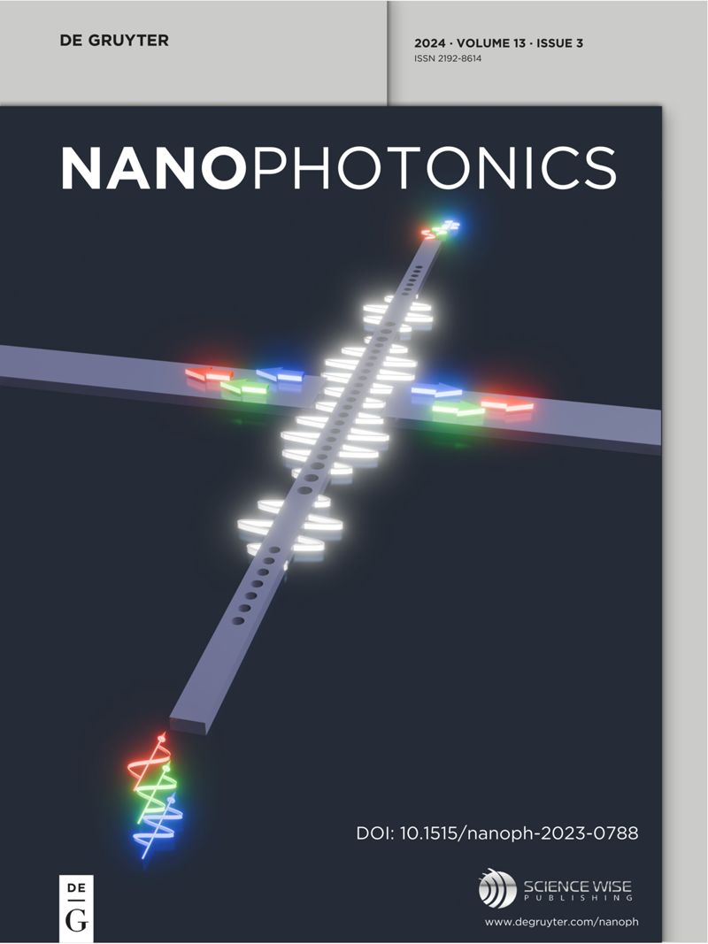
Nanophotonics
Nanophotonics NANOSCIENCE & NANOTECHNOLOGY-MATERIALS SCIENCE, MULTIDISCIPLINARY
CiteScore
13.50
自引率
6.70%
发文量
358
审稿时长
7 weeks
期刊介绍: Nanophotonics, published in collaboration with Sciencewise, is a prestigious journal that showcases recent international research results, notable advancements in the field, and innovative applications. It is regarded as one of the leading publications in the realm of nanophotonics and encompasses a range of article types including research articles, selectively invited reviews, letters, and perspectives. The journal specifically delves into the study of photon interaction with nano-structures, such as carbon nano-tubes, nano metal particles, nano crystals, semiconductor nano dots, photonic crystals, tissue, and DNA. It offers comprehensive coverage of the most up-to-date discoveries, making it an essential resource for physicists, engineers, and material scientists.
×
引用
GB/T 7714-2015
复制
MLA
复制
APA
复制
导出至
BibTeX EndNote RefMan NoteFirst NoteExpress
×
提示
您的信息不完整,为了账户安全,请先补充。
现在去补充
×
提示
您因"违规操作"
具体请查看互助需知
我知道了
×
提示
确定
请完成安全验证×
copy
已复制链接
快去分享给好友吧!
我知道了
右上角分享
点击右上角分享
0
联系我们:info@booksci.cn Book学术提供免费学术资源搜索服务,方便国内外学者检索中英文文献。致力于提供最便捷和优质的服务体验。 Copyright © 2023 布克学术 All rights reserved.
京ICP备2023020795号-1
ghs 京公网安备 11010802042870号
Book学术文献互助
Book学术文献互助群
群 号:481959085
Book学术官方微信