Sourav Rudra, Dheemahi Rao, Samuel Poncé, Bivas Saha
{"title":"限制氮化钪电子迁移率的主要散射机制","authors":"Sourav Rudra, Dheemahi Rao, Samuel Poncé, Bivas Saha","doi":"10.1021/acs.nanolett.4c02920","DOIUrl":null,"url":null,"abstract":"<p><p>Electron mobility in nitride semiconductors is limited by electron-phonon, defect, grain-boundary, and dislocation scatterings. Scandium nitride (ScN), an emerging rocksalt indirect bandgap semiconductor, exhibits varying electron mobilities depending on growth conditions. Since achieving high mobility is crucial for ScN's device applications, a microscopic understanding of different scattering mechanisms is extremely important. Utilizing the <i>ab initio</i> Boltzmann transport formalism and experimental measurements, here we show the hierarchy of various scattering processes in restricting the electron mobility of ScN. Calculations unveil that though Fröhlich interactions set an intrinsic upper bound for ScN's electron mobility of ∼524 cm<sup>2</sup>/V·s at room temperature, ionized-impurity and grain-boundary scatterings significantly reduce mobility. The experimental temperature dependence of mobilities is captured well considering both nitrogen-vacancy and oxygen-substitutional impurities with appropriate ratios, and room-temperature doping dependency agrees well with the empirical Caughey-Thomas model. Furthermore, we suggest modulation doping and polar-discontinuity doping to reduce ionized-impurity scattering in achieving a high-mobility ScN for device applications.</p>","PeriodicalId":53,"journal":{"name":"Nano Letters","volume":null,"pages":null},"PeriodicalIF":9.6000,"publicationDate":"2024-09-18","publicationTypes":"Journal Article","fieldsOfStudy":null,"isOpenAccess":false,"openAccessPdf":"","citationCount":"0","resultStr":"{\"title\":\"Dominant Scattering Mechanisms in Limiting the Electron Mobility of Scandium Nitride.\",\"authors\":\"Sourav Rudra, Dheemahi Rao, Samuel Poncé, Bivas Saha\",\"doi\":\"10.1021/acs.nanolett.4c02920\",\"DOIUrl\":null,\"url\":null,\"abstract\":\"<p><p>Electron mobility in nitride semiconductors is limited by electron-phonon, defect, grain-boundary, and dislocation scatterings. Scandium nitride (ScN), an emerging rocksalt indirect bandgap semiconductor, exhibits varying electron mobilities depending on growth conditions. Since achieving high mobility is crucial for ScN's device applications, a microscopic understanding of different scattering mechanisms is extremely important. Utilizing the <i>ab initio</i> Boltzmann transport formalism and experimental measurements, here we show the hierarchy of various scattering processes in restricting the electron mobility of ScN. Calculations unveil that though Fröhlich interactions set an intrinsic upper bound for ScN's electron mobility of ∼524 cm<sup>2</sup>/V·s at room temperature, ionized-impurity and grain-boundary scatterings significantly reduce mobility. The experimental temperature dependence of mobilities is captured well considering both nitrogen-vacancy and oxygen-substitutional impurities with appropriate ratios, and room-temperature doping dependency agrees well with the empirical Caughey-Thomas model. Furthermore, we suggest modulation doping and polar-discontinuity doping to reduce ionized-impurity scattering in achieving a high-mobility ScN for device applications.</p>\",\"PeriodicalId\":53,\"journal\":{\"name\":\"Nano Letters\",\"volume\":null,\"pages\":null},\"PeriodicalIF\":9.6000,\"publicationDate\":\"2024-09-18\",\"publicationTypes\":\"Journal Article\",\"fieldsOfStudy\":null,\"isOpenAccess\":false,\"openAccessPdf\":\"\",\"citationCount\":\"0\",\"resultStr\":null,\"platform\":\"Semanticscholar\",\"paperid\":null,\"PeriodicalName\":\"Nano Letters\",\"FirstCategoryId\":\"88\",\"ListUrlMain\":\"https://doi.org/10.1021/acs.nanolett.4c02920\",\"RegionNum\":1,\"RegionCategory\":\"材料科学\",\"ArticlePicture\":[],\"TitleCN\":null,\"AbstractTextCN\":null,\"PMCID\":null,\"EPubDate\":\"2024/9/6 0:00:00\",\"PubModel\":\"Epub\",\"JCR\":\"Q1\",\"JCRName\":\"CHEMISTRY, MULTIDISCIPLINARY\",\"Score\":null,\"Total\":0}","platform":"Semanticscholar","paperid":null,"PeriodicalName":"Nano Letters","FirstCategoryId":"88","ListUrlMain":"https://doi.org/10.1021/acs.nanolett.4c02920","RegionNum":1,"RegionCategory":"材料科学","ArticlePicture":[],"TitleCN":null,"AbstractTextCN":null,"PMCID":null,"EPubDate":"2024/9/6 0:00:00","PubModel":"Epub","JCR":"Q1","JCRName":"CHEMISTRY, MULTIDISCIPLINARY","Score":null,"Total":0}
引用次数: 0
摘要
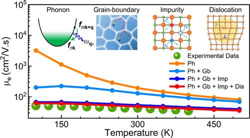
氮化物半导体中的电子迁移率受到电子-声子、缺陷、晶界和位错散射的限制。氮化钪(ScN)是一种新兴的岩盐间接带隙半导体,其电子迁移率因生长条件而异。由于实现高迁移率对 ScN 的器件应用至关重要,因此从微观上了解不同的散射机制极为重要。在此,我们利用 Ab initio Boltzmann 传输形式主义和实验测量结果,展示了各种散射过程在限制 ScN 电子迁移率方面的层次结构。计算结果表明,尽管弗洛里希相互作用为室温下的 ScN 电子迁移率设定了 ∼524 cm2/V-s 的固有上限,但电离杂质和晶界散射会显著降低迁移率。考虑到氮空位和氧置换杂质的适当比例,迁移率的实验温度依赖性得到了很好的捕捉,室温掺杂依赖性与经验考奇-托马斯模型非常吻合。此外,我们还建议采用调制掺杂和极性不连续掺杂来减少电离杂质散射,以实现器件应用中的高迁移率 ScN。
Dominant Scattering Mechanisms in Limiting the Electron Mobility of Scandium Nitride.
Electron mobility in nitride semiconductors is limited by electron-phonon, defect, grain-boundary, and dislocation scatterings. Scandium nitride (ScN), an emerging rocksalt indirect bandgap semiconductor, exhibits varying electron mobilities depending on growth conditions. Since achieving high mobility is crucial for ScN's device applications, a microscopic understanding of different scattering mechanisms is extremely important. Utilizing the ab initio Boltzmann transport formalism and experimental measurements, here we show the hierarchy of various scattering processes in restricting the electron mobility of ScN. Calculations unveil that though Fröhlich interactions set an intrinsic upper bound for ScN's electron mobility of ∼524 cm2/V·s at room temperature, ionized-impurity and grain-boundary scatterings significantly reduce mobility. The experimental temperature dependence of mobilities is captured well considering both nitrogen-vacancy and oxygen-substitutional impurities with appropriate ratios, and room-temperature doping dependency agrees well with the empirical Caughey-Thomas model. Furthermore, we suggest modulation doping and polar-discontinuity doping to reduce ionized-impurity scattering in achieving a high-mobility ScN for device applications.
期刊介绍:
Nano Letters serves as a dynamic platform for promptly disseminating original results in fundamental, applied, and emerging research across all facets of nanoscience and nanotechnology. A pivotal criterion for inclusion within Nano Letters is the convergence of at least two different areas or disciplines, ensuring a rich interdisciplinary scope. The journal is dedicated to fostering exploration in diverse areas, including:
- Experimental and theoretical findings on physical, chemical, and biological phenomena at the nanoscale
- Synthesis, characterization, and processing of organic, inorganic, polymer, and hybrid nanomaterials through physical, chemical, and biological methodologies
- Modeling and simulation of synthetic, assembly, and interaction processes
- Realization of integrated nanostructures and nano-engineered devices exhibiting advanced performance
- Applications of nanoscale materials in living and environmental systems
Nano Letters is committed to advancing and showcasing groundbreaking research that intersects various domains, fostering innovation and collaboration in the ever-evolving field of nanoscience and nanotechnology.

 求助内容:
求助内容: 应助结果提醒方式:


