Eduardo Granados, Miguel Martinez-Calderon, Baptiste Groussin, Jean Philippe Colombier, Ibon Santiago
{"title":"利用深紫外飞秒脉冲实现高度均匀的硅纳米图案化","authors":"Eduardo Granados, Miguel Martinez-Calderon, Baptiste Groussin, Jean Philippe Colombier, Ibon Santiago","doi":"10.1515/nanoph-2024-0240","DOIUrl":null,"url":null,"abstract":"The prospect of employing nanophotonic methods for controlling photon–electron interactions has ignited substantial interest within the particle accelerator community. Silicon-based integrated dielectric laser acceleration (DLA) has emerged as a viable option by leveraging localized photonic effects to emit, accelerate, and measure electron bunches using exclusively light. Here, using highly regular nanopatterning over large areas while preserving the crystalline structure of silicon is imperative to enhance the efficiency and yield of photon-electron effects. While several established fabrication techniques may be used to produce the required silicon nanostructures, alternative techniques are beneficial to enhance scalability, simplicity and cost-efficiency. In this study, we demonstrate the nano-synthesis of silicon structures over arbitrarily large areas utilizing exclusively deep ultraviolet (DUV) ultrafast laser excitation. This approach delivers highly concentrated electromagnetic energy to the material, thus producing nanostructures with features well beyond the diffraction limit. At the core of our demonstration is the production of silicon laser-induced surface structures with an exceptionally high aspect-ratio -reaching a height of more than 100 nm- for a nanostructure periodicity of 250 nm. This result is attained by exploiting a positive feedback effect on the locally enhanced laser electric field as the surface morphology dynamically emerges, in combination with the material properties at DUV wavelengths. We also observe strong nanopattern hybridization yielding intricate 2D structural features as the onset of amorphization takes place at high laser pulse fluence. This technique offers a simple, yet efficient and attractive approach to produce highly uniform and high aspect ratio silicon nanostructures in the 200–300 nm range.","PeriodicalId":19027,"journal":{"name":"Nanophotonics","volume":"101 1","pages":""},"PeriodicalIF":6.5000,"publicationDate":"2024-09-04","publicationTypes":"Journal Article","fieldsOfStudy":null,"isOpenAccess":false,"openAccessPdf":"","citationCount":"0","resultStr":"{\"title\":\"Highly uniform silicon nanopatterning with deep-ultraviolet femtosecond pulses\",\"authors\":\"Eduardo Granados, Miguel Martinez-Calderon, Baptiste Groussin, Jean Philippe Colombier, Ibon Santiago\",\"doi\":\"10.1515/nanoph-2024-0240\",\"DOIUrl\":null,\"url\":null,\"abstract\":\"The prospect of employing nanophotonic methods for controlling photon–electron interactions has ignited substantial interest within the particle accelerator community. Silicon-based integrated dielectric laser acceleration (DLA) has emerged as a viable option by leveraging localized photonic effects to emit, accelerate, and measure electron bunches using exclusively light. Here, using highly regular nanopatterning over large areas while preserving the crystalline structure of silicon is imperative to enhance the efficiency and yield of photon-electron effects. While several established fabrication techniques may be used to produce the required silicon nanostructures, alternative techniques are beneficial to enhance scalability, simplicity and cost-efficiency. In this study, we demonstrate the nano-synthesis of silicon structures over arbitrarily large areas utilizing exclusively deep ultraviolet (DUV) ultrafast laser excitation. This approach delivers highly concentrated electromagnetic energy to the material, thus producing nanostructures with features well beyond the diffraction limit. At the core of our demonstration is the production of silicon laser-induced surface structures with an exceptionally high aspect-ratio -reaching a height of more than 100 nm- for a nanostructure periodicity of 250 nm. This result is attained by exploiting a positive feedback effect on the locally enhanced laser electric field as the surface morphology dynamically emerges, in combination with the material properties at DUV wavelengths. We also observe strong nanopattern hybridization yielding intricate 2D structural features as the onset of amorphization takes place at high laser pulse fluence. This technique offers a simple, yet efficient and attractive approach to produce highly uniform and high aspect ratio silicon nanostructures in the 200–300 nm range.\",\"PeriodicalId\":19027,\"journal\":{\"name\":\"Nanophotonics\",\"volume\":\"101 1\",\"pages\":\"\"},\"PeriodicalIF\":6.5000,\"publicationDate\":\"2024-09-04\",\"publicationTypes\":\"Journal Article\",\"fieldsOfStudy\":null,\"isOpenAccess\":false,\"openAccessPdf\":\"\",\"citationCount\":\"0\",\"resultStr\":null,\"platform\":\"Semanticscholar\",\"paperid\":null,\"PeriodicalName\":\"Nanophotonics\",\"FirstCategoryId\":\"101\",\"ListUrlMain\":\"https://doi.org/10.1515/nanoph-2024-0240\",\"RegionNum\":2,\"RegionCategory\":\"物理与天体物理\",\"ArticlePicture\":[],\"TitleCN\":null,\"AbstractTextCN\":null,\"PMCID\":null,\"EPubDate\":\"\",\"PubModel\":\"\",\"JCR\":\"Q1\",\"JCRName\":\"MATERIALS SCIENCE, MULTIDISCIPLINARY\",\"Score\":null,\"Total\":0}","platform":"Semanticscholar","paperid":null,"PeriodicalName":"Nanophotonics","FirstCategoryId":"101","ListUrlMain":"https://doi.org/10.1515/nanoph-2024-0240","RegionNum":2,"RegionCategory":"物理与天体物理","ArticlePicture":[],"TitleCN":null,"AbstractTextCN":null,"PMCID":null,"EPubDate":"","PubModel":"","JCR":"Q1","JCRName":"MATERIALS SCIENCE, MULTIDISCIPLINARY","Score":null,"Total":0}
Highly uniform silicon nanopatterning with deep-ultraviolet femtosecond pulses
The prospect of employing nanophotonic methods for controlling photon–electron interactions has ignited substantial interest within the particle accelerator community. Silicon-based integrated dielectric laser acceleration (DLA) has emerged as a viable option by leveraging localized photonic effects to emit, accelerate, and measure electron bunches using exclusively light. Here, using highly regular nanopatterning over large areas while preserving the crystalline structure of silicon is imperative to enhance the efficiency and yield of photon-electron effects. While several established fabrication techniques may be used to produce the required silicon nanostructures, alternative techniques are beneficial to enhance scalability, simplicity and cost-efficiency. In this study, we demonstrate the nano-synthesis of silicon structures over arbitrarily large areas utilizing exclusively deep ultraviolet (DUV) ultrafast laser excitation. This approach delivers highly concentrated electromagnetic energy to the material, thus producing nanostructures with features well beyond the diffraction limit. At the core of our demonstration is the production of silicon laser-induced surface structures with an exceptionally high aspect-ratio -reaching a height of more than 100 nm- for a nanostructure periodicity of 250 nm. This result is attained by exploiting a positive feedback effect on the locally enhanced laser electric field as the surface morphology dynamically emerges, in combination with the material properties at DUV wavelengths. We also observe strong nanopattern hybridization yielding intricate 2D structural features as the onset of amorphization takes place at high laser pulse fluence. This technique offers a simple, yet efficient and attractive approach to produce highly uniform and high aspect ratio silicon nanostructures in the 200–300 nm range.
期刊介绍:
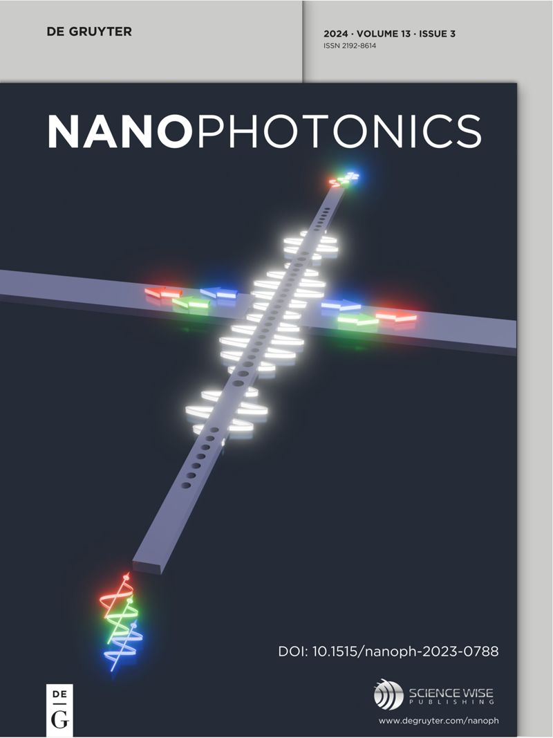
Nanophotonics, published in collaboration with Sciencewise, is a prestigious journal that showcases recent international research results, notable advancements in the field, and innovative applications. It is regarded as one of the leading publications in the realm of nanophotonics and encompasses a range of article types including research articles, selectively invited reviews, letters, and perspectives.
The journal specifically delves into the study of photon interaction with nano-structures, such as carbon nano-tubes, nano metal particles, nano crystals, semiconductor nano dots, photonic crystals, tissue, and DNA. It offers comprehensive coverage of the most up-to-date discoveries, making it an essential resource for physicists, engineers, and material scientists.