{"title":"通过图案化基底工程实现具有周期性应变的纳米图案化单层 MoS2 的共形生长,从而实现高性能光电探测器","authors":"Pengcheng Jian, Maohua Chen, Dongyan Li, Yongming Zhao, Weijie Liu, Yuang Luo, Xiantai Tian, Meng Peng, Xing Zhou, Jiangnan Dai, Feng Wu, Changqing Chen","doi":"10.1002/lpor.202401012","DOIUrl":null,"url":null,"abstract":"<p>The extraordinary mechanical compliance of 2D molybdenum disulfide (MoS<sub>2</sub>) makes it an ideal candidate for strain modulation of various electrical and optical properties. However, developing facile methods for accurate and stable engineering of strain still remains a major challenge. Here, a novel and effective method is demonstrated for introducing periodic strain into monolayer MoS<sub>2</sub> by direct growth on nano-patterned sapphire substrates (NPSS). A mixed aqueous solution of Na<sub>2</sub>MoO<sub>4</sub> and NaOH is spin-coated on the NPSS and sulfurated in one step by chemical vapor deposition (CVD). Highly oriented monolayer MoS<sub>2</sub> single-crystal nanosheets with high quality and few sulfur vacancies are achieved conformally on the NPSS via a liquid-mediated growth mode. Notably, the periodically distributed blue shift of the PL emission peak demonstrated periodic compressive strain is introduced into the nano-patterned MoS<sub>2</sub> via the thermal expansion difference between MoS<sub>2</sub> and substrates. Furthermore, photodetectors fabricated using the nano-patterned monolayer MoS<sub>2</sub> exhibit a high photo-to-dark current ratio (PDCR) over 10<sup>6</sup>, an excellent detectivity of 5.4 × 10<sup>13</sup> Jones, and a fast photoresponse of 7.7 ms, owing to the strain-induced back-to-back built-in electric field, enhanced light absorption by light-scattering effect and fewer S vacancy defects. The scanning imaging demonstration based on the single-pixel nano-patterned MoS<sub>2</sub> photodetector further confirms its great potential in image sensors. This work hereby presents a pathway for direct conformal growth of nano-patterned monolayer MoS<sub>2</sub> with precisely periodic strain, which should inspire the applications for high-performance optoelectronic devices via the strategy of patterned substrate engineering by the periodic nanostructures.</p>","PeriodicalId":204,"journal":{"name":"Laser & Photonics Reviews","volume":"19 1","pages":""},"PeriodicalIF":9.8000,"publicationDate":"2024-08-30","publicationTypes":"Journal Article","fieldsOfStudy":null,"isOpenAccess":false,"openAccessPdf":"","citationCount":"0","resultStr":"{\"title\":\"Conformal Growth of Nano-Patterned Monolayer MoS2 with Periodic Strain via Patterned Substrate Engineering for High-performance Photodetectors\",\"authors\":\"Pengcheng Jian, Maohua Chen, Dongyan Li, Yongming Zhao, Weijie Liu, Yuang Luo, Xiantai Tian, Meng Peng, Xing Zhou, Jiangnan Dai, Feng Wu, Changqing Chen\",\"doi\":\"10.1002/lpor.202401012\",\"DOIUrl\":null,\"url\":null,\"abstract\":\"<p>The extraordinary mechanical compliance of 2D molybdenum disulfide (MoS<sub>2</sub>) makes it an ideal candidate for strain modulation of various electrical and optical properties. However, developing facile methods for accurate and stable engineering of strain still remains a major challenge. Here, a novel and effective method is demonstrated for introducing periodic strain into monolayer MoS<sub>2</sub> by direct growth on nano-patterned sapphire substrates (NPSS). A mixed aqueous solution of Na<sub>2</sub>MoO<sub>4</sub> and NaOH is spin-coated on the NPSS and sulfurated in one step by chemical vapor deposition (CVD). Highly oriented monolayer MoS<sub>2</sub> single-crystal nanosheets with high quality and few sulfur vacancies are achieved conformally on the NPSS via a liquid-mediated growth mode. Notably, the periodically distributed blue shift of the PL emission peak demonstrated periodic compressive strain is introduced into the nano-patterned MoS<sub>2</sub> via the thermal expansion difference between MoS<sub>2</sub> and substrates. Furthermore, photodetectors fabricated using the nano-patterned monolayer MoS<sub>2</sub> exhibit a high photo-to-dark current ratio (PDCR) over 10<sup>6</sup>, an excellent detectivity of 5.4 × 10<sup>13</sup> Jones, and a fast photoresponse of 7.7 ms, owing to the strain-induced back-to-back built-in electric field, enhanced light absorption by light-scattering effect and fewer S vacancy defects. The scanning imaging demonstration based on the single-pixel nano-patterned MoS<sub>2</sub> photodetector further confirms its great potential in image sensors. This work hereby presents a pathway for direct conformal growth of nano-patterned monolayer MoS<sub>2</sub> with precisely periodic strain, which should inspire the applications for high-performance optoelectronic devices via the strategy of patterned substrate engineering by the periodic nanostructures.</p>\",\"PeriodicalId\":204,\"journal\":{\"name\":\"Laser & Photonics Reviews\",\"volume\":\"19 1\",\"pages\":\"\"},\"PeriodicalIF\":9.8000,\"publicationDate\":\"2024-08-30\",\"publicationTypes\":\"Journal Article\",\"fieldsOfStudy\":null,\"isOpenAccess\":false,\"openAccessPdf\":\"\",\"citationCount\":\"0\",\"resultStr\":null,\"platform\":\"Semanticscholar\",\"paperid\":null,\"PeriodicalName\":\"Laser & Photonics Reviews\",\"FirstCategoryId\":\"101\",\"ListUrlMain\":\"https://onlinelibrary.wiley.com/doi/10.1002/lpor.202401012\",\"RegionNum\":1,\"RegionCategory\":\"物理与天体物理\",\"ArticlePicture\":[],\"TitleCN\":null,\"AbstractTextCN\":null,\"PMCID\":null,\"EPubDate\":\"\",\"PubModel\":\"\",\"JCR\":\"Q1\",\"JCRName\":\"OPTICS\",\"Score\":null,\"Total\":0}","platform":"Semanticscholar","paperid":null,"PeriodicalName":"Laser & Photonics Reviews","FirstCategoryId":"101","ListUrlMain":"https://onlinelibrary.wiley.com/doi/10.1002/lpor.202401012","RegionNum":1,"RegionCategory":"物理与天体物理","ArticlePicture":[],"TitleCN":null,"AbstractTextCN":null,"PMCID":null,"EPubDate":"","PubModel":"","JCR":"Q1","JCRName":"OPTICS","Score":null,"Total":0}
Conformal Growth of Nano-Patterned Monolayer MoS2 with Periodic Strain via Patterned Substrate Engineering for High-performance Photodetectors
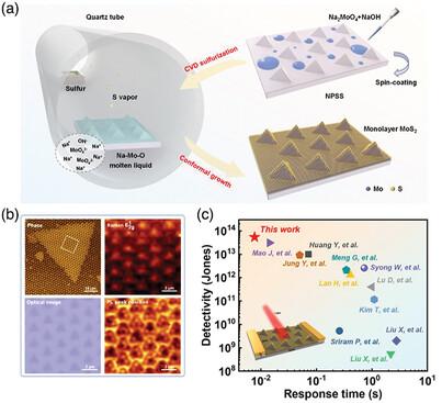
The extraordinary mechanical compliance of 2D molybdenum disulfide (MoS2) makes it an ideal candidate for strain modulation of various electrical and optical properties. However, developing facile methods for accurate and stable engineering of strain still remains a major challenge. Here, a novel and effective method is demonstrated for introducing periodic strain into monolayer MoS2 by direct growth on nano-patterned sapphire substrates (NPSS). A mixed aqueous solution of Na2MoO4 and NaOH is spin-coated on the NPSS and sulfurated in one step by chemical vapor deposition (CVD). Highly oriented monolayer MoS2 single-crystal nanosheets with high quality and few sulfur vacancies are achieved conformally on the NPSS via a liquid-mediated growth mode. Notably, the periodically distributed blue shift of the PL emission peak demonstrated periodic compressive strain is introduced into the nano-patterned MoS2 via the thermal expansion difference between MoS2 and substrates. Furthermore, photodetectors fabricated using the nano-patterned monolayer MoS2 exhibit a high photo-to-dark current ratio (PDCR) over 106, an excellent detectivity of 5.4 × 10¹³ Jones, and a fast photoresponse of 7.7 ms, owing to the strain-induced back-to-back built-in electric field, enhanced light absorption by light-scattering effect and fewer S vacancy defects. The scanning imaging demonstration based on the single-pixel nano-patterned MoS2 photodetector further confirms its great potential in image sensors. This work hereby presents a pathway for direct conformal growth of nano-patterned monolayer MoS2 with precisely periodic strain, which should inspire the applications for high-performance optoelectronic devices via the strategy of patterned substrate engineering by the periodic nanostructures.
期刊介绍:
Laser & Photonics Reviews is a reputable journal that publishes high-quality Reviews, original Research Articles, and Perspectives in the field of photonics and optics. It covers both theoretical and experimental aspects, including recent groundbreaking research, specific advancements, and innovative applications.
As evidence of its impact and recognition, Laser & Photonics Reviews boasts a remarkable 2022 Impact Factor of 11.0, according to the Journal Citation Reports from Clarivate Analytics (2023). Moreover, it holds impressive rankings in the InCites Journal Citation Reports: in 2021, it was ranked 6th out of 101 in the field of Optics, 15th out of 161 in Applied Physics, and 12th out of 69 in Condensed Matter Physics.
The journal uses the ISSN numbers 1863-8880 for print and 1863-8899 for online publications.

 求助内容:
求助内容: 应助结果提醒方式:


