Jeetendra Gour, Sebastian Beer, Pallabi Paul, Alessandro Alberucci, Michael Steinert, Adriana Szeghalmi, Thomas Siefke, Ulf Peschel, Stefan Nolte, Uwe Detlef Zeitner
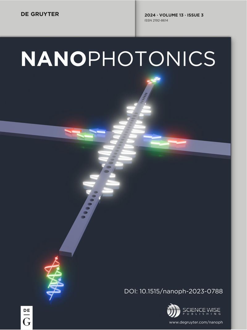
{"title":"晶圆级纳米制造 5 纳米以下的等离子体元表面间隙","authors":"Jeetendra Gour, Sebastian Beer, Pallabi Paul, Alessandro Alberucci, Michael Steinert, Adriana Szeghalmi, Thomas Siefke, Ulf Peschel, Stefan Nolte, Uwe Detlef Zeitner","doi":"10.1515/nanoph-2024-0343","DOIUrl":null,"url":null,"abstract":"In the rapidly evolving field of plasmonic metasurfaces, achieving homogeneous, reliable, and reproducible fabrication of sub-5 nm dielectric nanogaps is a significant challenge. This article presents an advanced fabrication technology that addresses this issue, capable of realizing uniform and reliable vertical nanogap metasurfaces on a whole wafer of 100 mm diameter. By leveraging fast patterning techniques, such as variable-shaped and character projection electron beam lithography (EBL), along with atomic layer deposition (ALD) for defining a few nanometer gaps with sub-nanometer precision, we have developed a flexible nanofabrication technology to achieve gaps as narrow as 2 nm in plasmonic nanoantennas. The quality of our structures is experimentally demonstrated by the observation of resonant localized and collective modes corresponding to the lattice, with Q-factors reaching up to 165. Our technological process opens up new and exciting opportunities to fabricate macroscopic devices harnessing the strong enhancement of light–matter interaction at the single nanometer scale.","PeriodicalId":19027,"journal":{"name":"Nanophotonics","volume":"30 1","pages":""},"PeriodicalIF":6.5000,"publicationDate":"2024-08-27","publicationTypes":"Journal Article","fieldsOfStudy":null,"isOpenAccess":false,"openAccessPdf":"","citationCount":"0","resultStr":"{\"title\":\"Wafer-scale nanofabrication of sub-5 nm gaps in plasmonic metasurfaces\",\"authors\":\"Jeetendra Gour, Sebastian Beer, Pallabi Paul, Alessandro Alberucci, Michael Steinert, Adriana Szeghalmi, Thomas Siefke, Ulf Peschel, Stefan Nolte, Uwe Detlef Zeitner\",\"doi\":\"10.1515/nanoph-2024-0343\",\"DOIUrl\":null,\"url\":null,\"abstract\":\"In the rapidly evolving field of plasmonic metasurfaces, achieving homogeneous, reliable, and reproducible fabrication of sub-5 nm dielectric nanogaps is a significant challenge. This article presents an advanced fabrication technology that addresses this issue, capable of realizing uniform and reliable vertical nanogap metasurfaces on a whole wafer of 100 mm diameter. By leveraging fast patterning techniques, such as variable-shaped and character projection electron beam lithography (EBL), along with atomic layer deposition (ALD) for defining a few nanometer gaps with sub-nanometer precision, we have developed a flexible nanofabrication technology to achieve gaps as narrow as 2 nm in plasmonic nanoantennas. The quality of our structures is experimentally demonstrated by the observation of resonant localized and collective modes corresponding to the lattice, with Q-factors reaching up to 165. Our technological process opens up new and exciting opportunities to fabricate macroscopic devices harnessing the strong enhancement of light–matter interaction at the single nanometer scale.\",\"PeriodicalId\":19027,\"journal\":{\"name\":\"Nanophotonics\",\"volume\":\"30 1\",\"pages\":\"\"},\"PeriodicalIF\":6.5000,\"publicationDate\":\"2024-08-27\",\"publicationTypes\":\"Journal Article\",\"fieldsOfStudy\":null,\"isOpenAccess\":false,\"openAccessPdf\":\"\",\"citationCount\":\"0\",\"resultStr\":null,\"platform\":\"Semanticscholar\",\"paperid\":null,\"PeriodicalName\":\"Nanophotonics\",\"FirstCategoryId\":\"101\",\"ListUrlMain\":\"https://doi.org/10.1515/nanoph-2024-0343\",\"RegionNum\":2,\"RegionCategory\":\"物理与天体物理\",\"ArticlePicture\":[],\"TitleCN\":null,\"AbstractTextCN\":null,\"PMCID\":null,\"EPubDate\":\"\",\"PubModel\":\"\",\"JCR\":\"Q1\",\"JCRName\":\"MATERIALS SCIENCE, MULTIDISCIPLINARY\",\"Score\":null,\"Total\":0}","platform":"Semanticscholar","paperid":null,"PeriodicalName":"Nanophotonics","FirstCategoryId":"101","ListUrlMain":"https://doi.org/10.1515/nanoph-2024-0343","RegionNum":2,"RegionCategory":"物理与天体物理","ArticlePicture":[],"TitleCN":null,"AbstractTextCN":null,"PMCID":null,"EPubDate":"","PubModel":"","JCR":"Q1","JCRName":"MATERIALS SCIENCE, MULTIDISCIPLINARY","Score":null,"Total":0}
Wafer-scale nanofabrication of sub-5 nm gaps in plasmonic metasurfaces
In the rapidly evolving field of plasmonic metasurfaces, achieving homogeneous, reliable, and reproducible fabrication of sub-5 nm dielectric nanogaps is a significant challenge. This article presents an advanced fabrication technology that addresses this issue, capable of realizing uniform and reliable vertical nanogap metasurfaces on a whole wafer of 100 mm diameter. By leveraging fast patterning techniques, such as variable-shaped and character projection electron beam lithography (EBL), along with atomic layer deposition (ALD) for defining a few nanometer gaps with sub-nanometer precision, we have developed a flexible nanofabrication technology to achieve gaps as narrow as 2 nm in plasmonic nanoantennas. The quality of our structures is experimentally demonstrated by the observation of resonant localized and collective modes corresponding to the lattice, with Q-factors reaching up to 165. Our technological process opens up new and exciting opportunities to fabricate macroscopic devices harnessing the strong enhancement of light–matter interaction at the single nanometer scale.
期刊介绍:
Nanophotonics, published in collaboration with Sciencewise, is a prestigious journal that showcases recent international research results, notable advancements in the field, and innovative applications. It is regarded as one of the leading publications in the realm of nanophotonics and encompasses a range of article types including research articles, selectively invited reviews, letters, and perspectives.
The journal specifically delves into the study of photon interaction with nano-structures, such as carbon nano-tubes, nano metal particles, nano crystals, semiconductor nano dots, photonic crystals, tissue, and DNA. It offers comprehensive coverage of the most up-to-date discoveries, making it an essential resource for physicists, engineers, and material scientists.