{"title":"利用蒙特卡罗模拟分析小型纳米级 MOSFET 中的 3D 沟道电流噪声。","authors":"Wenpeng Zhang, Qun Wei, Xiaofei Jia, Liang He","doi":"10.3390/nano14161359","DOIUrl":null,"url":null,"abstract":"<p><p>As field effect transistors are reduced to nanometer dimensions, experimental and theoretical research has shown a gradual change in noise generation mechanisms. There are few studies on noise theory for small nanoscale transistors, and Monte Carlo (MC) simulations mainly focus on 2D devices with larger nanoscale dimensions. In this study, we employed MC simulation techniques to establish a 3D device simulation process. By setting device parameters and writing simulation programs, we simulated the raw data of channel current noise for a silicon-based metal-oxide-semiconductor field-effect transistor (MOSFET) with a 10 nm channel length and calculated the drain output current based on these data, thereby achieving static testing of the simulated device. Additionally, this study obtained a 3D potential distribution map of the device channel surface area. Based on the original data from the simulation analysis, this study further calculated the power spectral density of the channel current noise and analyzed how the channel current noise varies with gate voltage, source-drain voltage, temperature, and substrate doping density. The results indicate that under low-temperature conditions, the channel current noise of the 10 nm MOSFET is primarily composed of suppressed shot noise, with the proportion of thermal noise in the total noise slightly increasing as temperature rises. Under normal operating conditions, the channel current noise characteristics of the 10 nm MOSFET device are jointly characterized by suppressed shot noise, thermal noise, and cross-correlated noise. Among these noise components, shot noise is the main source of noise, and its suppression degree decreases as the bias voltage is reduced. These findings are consistent with experimental observations and theoretical analyses found in the existing literature.</p>","PeriodicalId":18966,"journal":{"name":"Nanomaterials","volume":"14 16","pages":""},"PeriodicalIF":4.3000,"publicationDate":"2024-08-18","publicationTypes":"Journal Article","fieldsOfStudy":null,"isOpenAccess":false,"openAccessPdf":"https://www.ncbi.nlm.nih.gov/pmc/articles/PMC11357296/pdf/","citationCount":"0","resultStr":"{\"title\":\"Analysis of 3D Channel Current Noise in Small Nanoscale MOSFETs Using Monte Carlo Simulation.\",\"authors\":\"Wenpeng Zhang, Qun Wei, Xiaofei Jia, Liang He\",\"doi\":\"10.3390/nano14161359\",\"DOIUrl\":null,\"url\":null,\"abstract\":\"<p><p>As field effect transistors are reduced to nanometer dimensions, experimental and theoretical research has shown a gradual change in noise generation mechanisms. There are few studies on noise theory for small nanoscale transistors, and Monte Carlo (MC) simulations mainly focus on 2D devices with larger nanoscale dimensions. In this study, we employed MC simulation techniques to establish a 3D device simulation process. By setting device parameters and writing simulation programs, we simulated the raw data of channel current noise for a silicon-based metal-oxide-semiconductor field-effect transistor (MOSFET) with a 10 nm channel length and calculated the drain output current based on these data, thereby achieving static testing of the simulated device. Additionally, this study obtained a 3D potential distribution map of the device channel surface area. Based on the original data from the simulation analysis, this study further calculated the power spectral density of the channel current noise and analyzed how the channel current noise varies with gate voltage, source-drain voltage, temperature, and substrate doping density. The results indicate that under low-temperature conditions, the channel current noise of the 10 nm MOSFET is primarily composed of suppressed shot noise, with the proportion of thermal noise in the total noise slightly increasing as temperature rises. Under normal operating conditions, the channel current noise characteristics of the 10 nm MOSFET device are jointly characterized by suppressed shot noise, thermal noise, and cross-correlated noise. Among these noise components, shot noise is the main source of noise, and its suppression degree decreases as the bias voltage is reduced. These findings are consistent with experimental observations and theoretical analyses found in the existing literature.</p>\",\"PeriodicalId\":18966,\"journal\":{\"name\":\"Nanomaterials\",\"volume\":\"14 16\",\"pages\":\"\"},\"PeriodicalIF\":4.3000,\"publicationDate\":\"2024-08-18\",\"publicationTypes\":\"Journal Article\",\"fieldsOfStudy\":null,\"isOpenAccess\":false,\"openAccessPdf\":\"https://www.ncbi.nlm.nih.gov/pmc/articles/PMC11357296/pdf/\",\"citationCount\":\"0\",\"resultStr\":null,\"platform\":\"Semanticscholar\",\"paperid\":null,\"PeriodicalName\":\"Nanomaterials\",\"FirstCategoryId\":\"88\",\"ListUrlMain\":\"https://doi.org/10.3390/nano14161359\",\"RegionNum\":3,\"RegionCategory\":\"材料科学\",\"ArticlePicture\":[],\"TitleCN\":null,\"AbstractTextCN\":null,\"PMCID\":null,\"EPubDate\":\"\",\"PubModel\":\"\",\"JCR\":\"Q2\",\"JCRName\":\"CHEMISTRY, MULTIDISCIPLINARY\",\"Score\":null,\"Total\":0}","platform":"Semanticscholar","paperid":null,"PeriodicalName":"Nanomaterials","FirstCategoryId":"88","ListUrlMain":"https://doi.org/10.3390/nano14161359","RegionNum":3,"RegionCategory":"材料科学","ArticlePicture":[],"TitleCN":null,"AbstractTextCN":null,"PMCID":null,"EPubDate":"","PubModel":"","JCR":"Q2","JCRName":"CHEMISTRY, MULTIDISCIPLINARY","Score":null,"Total":0}
Analysis of 3D Channel Current Noise in Small Nanoscale MOSFETs Using Monte Carlo Simulation.
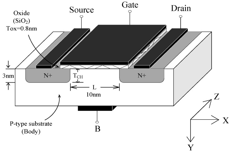
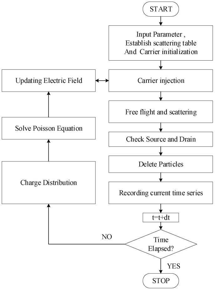
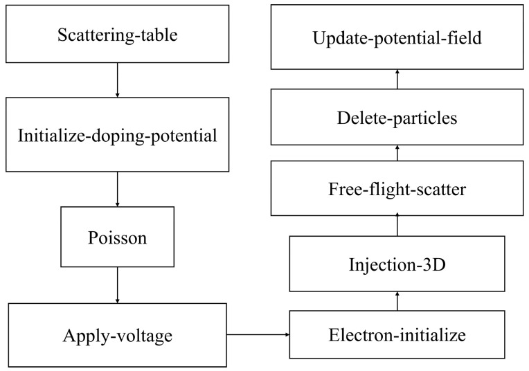
As field effect transistors are reduced to nanometer dimensions, experimental and theoretical research has shown a gradual change in noise generation mechanisms. There are few studies on noise theory for small nanoscale transistors, and Monte Carlo (MC) simulations mainly focus on 2D devices with larger nanoscale dimensions. In this study, we employed MC simulation techniques to establish a 3D device simulation process. By setting device parameters and writing simulation programs, we simulated the raw data of channel current noise for a silicon-based metal-oxide-semiconductor field-effect transistor (MOSFET) with a 10 nm channel length and calculated the drain output current based on these data, thereby achieving static testing of the simulated device. Additionally, this study obtained a 3D potential distribution map of the device channel surface area. Based on the original data from the simulation analysis, this study further calculated the power spectral density of the channel current noise and analyzed how the channel current noise varies with gate voltage, source-drain voltage, temperature, and substrate doping density. The results indicate that under low-temperature conditions, the channel current noise of the 10 nm MOSFET is primarily composed of suppressed shot noise, with the proportion of thermal noise in the total noise slightly increasing as temperature rises. Under normal operating conditions, the channel current noise characteristics of the 10 nm MOSFET device are jointly characterized by suppressed shot noise, thermal noise, and cross-correlated noise. Among these noise components, shot noise is the main source of noise, and its suppression degree decreases as the bias voltage is reduced. These findings are consistent with experimental observations and theoretical analyses found in the existing literature.
期刊介绍:
Nanomaterials (ISSN 2076-4991) is an international and interdisciplinary scholarly open access journal. It publishes reviews, regular research papers, communications, and short notes that are relevant to any field of study that involves nanomaterials, with respect to their science and application. Thus, theoretical and experimental articles will be accepted, along with articles that deal with the synthesis and use of nanomaterials. Articles that synthesize information from multiple fields, and which place discoveries within a broader context, will be preferred. There is no restriction on the length of the papers. Our aim is to encourage scientists to publish their experimental and theoretical research in as much detail as possible. Full experimental or methodical details, or both, must be provided for research articles. Computed data or files regarding the full details of the experimental procedure, if unable to be published in a normal way, can be deposited as supplementary material. Nanomaterials is dedicated to a high scientific standard. All manuscripts undergo a rigorous reviewing process and decisions are based on the recommendations of independent reviewers.

 求助内容:
求助内容: 应助结果提醒方式:


