Shivangi Srivastava, Anand Kumar Rai, Mayank Shrivastava and Praveen C. Ramamurthy*,
{"title":"通过优化电子束诱导交联的剂量,对 P3HT 进行 100 纳米以下的图案化,从而提高 OFET 器件的性能","authors":"Shivangi Srivastava, Anand Kumar Rai, Mayank Shrivastava and Praveen C. Ramamurthy*, ","doi":"10.1021/acsaelm.4c0090410.1021/acsaelm.4c00904","DOIUrl":null,"url":null,"abstract":"<p >Poly(3-hexylthiophene) (P3HT) has been extensively utilized as a p-type semiconductor material in organic electronics for numerous years. The patterning of P3HT is essential for various applications, including addressable sensor arrays, complementary logic circuits, and RFID tags. This process not only mitigates crosstalk between adjacent transistors but also enhances device speed and reduces parasitic capacitances. However, patterning P3HT poses significant challenges due to its incompatibility with various resists commonly employed in lithographic processes, which can lead to performance degradation in P3HT-based devices. This study addresses these issues by employing the electron beam-induced cross-linking (EBIC) method. This technique allows for the patterning of P3HT without the need for conventional preprocessing elements such as resists. Dose values of moderate beam energy were optimized to circumvent any potential performance degradation during the patterning process. These advancements have significantly enhanced the performance of organic field-effect transistors (OFETs) by increasing the I<sub>ON</sub>/I<sub>OFF</sub> ratio by about 6 orders of magnitude, reducing the subthreshold swing, and decreasing the interface trap density by an order of magnitude. This work presents a direct and efficacious approach to pattern P3HT-based OFETs, demonstrating their substantial potential to overcome challenges in polymer patterning, reduce device dimensions, and improve overall device performance.</p>","PeriodicalId":3,"journal":{"name":"ACS Applied Electronic Materials","volume":"6 8","pages":"5923–5933 5923–5933"},"PeriodicalIF":4.7000,"publicationDate":"2024-08-13","publicationTypes":"Journal Article","fieldsOfStudy":null,"isOpenAccess":false,"openAccessPdf":"","citationCount":"0","resultStr":"{\"title\":\"Sub-100 nm Patterning of P3HT with Enhanced OFET Device Performance by Dose Optimization of Electron Beam-Induced Cross-Linking\",\"authors\":\"Shivangi Srivastava, Anand Kumar Rai, Mayank Shrivastava and Praveen C. Ramamurthy*, \",\"doi\":\"10.1021/acsaelm.4c0090410.1021/acsaelm.4c00904\",\"DOIUrl\":null,\"url\":null,\"abstract\":\"<p >Poly(3-hexylthiophene) (P3HT) has been extensively utilized as a p-type semiconductor material in organic electronics for numerous years. The patterning of P3HT is essential for various applications, including addressable sensor arrays, complementary logic circuits, and RFID tags. This process not only mitigates crosstalk between adjacent transistors but also enhances device speed and reduces parasitic capacitances. However, patterning P3HT poses significant challenges due to its incompatibility with various resists commonly employed in lithographic processes, which can lead to performance degradation in P3HT-based devices. This study addresses these issues by employing the electron beam-induced cross-linking (EBIC) method. This technique allows for the patterning of P3HT without the need for conventional preprocessing elements such as resists. Dose values of moderate beam energy were optimized to circumvent any potential performance degradation during the patterning process. These advancements have significantly enhanced the performance of organic field-effect transistors (OFETs) by increasing the I<sub>ON</sub>/I<sub>OFF</sub> ratio by about 6 orders of magnitude, reducing the subthreshold swing, and decreasing the interface trap density by an order of magnitude. This work presents a direct and efficacious approach to pattern P3HT-based OFETs, demonstrating their substantial potential to overcome challenges in polymer patterning, reduce device dimensions, and improve overall device performance.</p>\",\"PeriodicalId\":3,\"journal\":{\"name\":\"ACS Applied Electronic Materials\",\"volume\":\"6 8\",\"pages\":\"5923–5933 5923–5933\"},\"PeriodicalIF\":4.7000,\"publicationDate\":\"2024-08-13\",\"publicationTypes\":\"Journal Article\",\"fieldsOfStudy\":null,\"isOpenAccess\":false,\"openAccessPdf\":\"\",\"citationCount\":\"0\",\"resultStr\":null,\"platform\":\"Semanticscholar\",\"paperid\":null,\"PeriodicalName\":\"ACS Applied Electronic Materials\",\"FirstCategoryId\":\"88\",\"ListUrlMain\":\"https://pubs.acs.org/doi/10.1021/acsaelm.4c00904\",\"RegionNum\":3,\"RegionCategory\":\"材料科学\",\"ArticlePicture\":[],\"TitleCN\":null,\"AbstractTextCN\":null,\"PMCID\":null,\"EPubDate\":\"\",\"PubModel\":\"\",\"JCR\":\"Q1\",\"JCRName\":\"ENGINEERING, ELECTRICAL & ELECTRONIC\",\"Score\":null,\"Total\":0}","platform":"Semanticscholar","paperid":null,"PeriodicalName":"ACS Applied Electronic Materials","FirstCategoryId":"88","ListUrlMain":"https://pubs.acs.org/doi/10.1021/acsaelm.4c00904","RegionNum":3,"RegionCategory":"材料科学","ArticlePicture":[],"TitleCN":null,"AbstractTextCN":null,"PMCID":null,"EPubDate":"","PubModel":"","JCR":"Q1","JCRName":"ENGINEERING, ELECTRICAL & ELECTRONIC","Score":null,"Total":0}
引用次数: 0
摘要
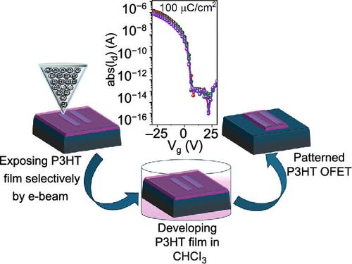
多年来,聚(3-己基噻吩)(P3HT)作为一种 p 型半导体材料被广泛应用于有机电子领域。P3HT 的图案化对于包括可寻址传感器阵列、互补逻辑电路和 RFID 标签在内的各种应用至关重要。这一工艺不仅能减少相邻晶体管之间的串扰,还能提高器件速度并减少寄生电容。然而,由于 P3HT 与光刻工艺中常用的各种抗蚀剂不兼容,导致基于 P3HT 的器件性能下降,因此图案化 P3HT 面临着巨大挑战。本研究采用电子束诱导交联(EBIC)方法解决了这些问题。该技术无需使用抗蚀剂等传统预处理元件,即可对 P3HT 进行图案化。对中等束能的剂量值进行了优化,以避免图案化过程中任何潜在的性能下降。这些进步大大提高了有机场效应晶体管(OFET)的性能,将离子/离子阱比提高了约 6 个数量级,减少了亚阈值摆动,并将界面阱密度降低了一个数量级。这项研究提出了一种直接有效的方法来对基于 P3HT 的 OFET 进行图案化,证明了其在克服聚合物图案化挑战、减小器件尺寸和提高器件整体性能方面的巨大潜力。
Sub-100 nm Patterning of P3HT with Enhanced OFET Device Performance by Dose Optimization of Electron Beam-Induced Cross-Linking
Poly(3-hexylthiophene) (P3HT) has been extensively utilized as a p-type semiconductor material in organic electronics for numerous years. The patterning of P3HT is essential for various applications, including addressable sensor arrays, complementary logic circuits, and RFID tags. This process not only mitigates crosstalk between adjacent transistors but also enhances device speed and reduces parasitic capacitances. However, patterning P3HT poses significant challenges due to its incompatibility with various resists commonly employed in lithographic processes, which can lead to performance degradation in P3HT-based devices. This study addresses these issues by employing the electron beam-induced cross-linking (EBIC) method. This technique allows for the patterning of P3HT without the need for conventional preprocessing elements such as resists. Dose values of moderate beam energy were optimized to circumvent any potential performance degradation during the patterning process. These advancements have significantly enhanced the performance of organic field-effect transistors (OFETs) by increasing the ION/IOFF ratio by about 6 orders of magnitude, reducing the subthreshold swing, and decreasing the interface trap density by an order of magnitude. This work presents a direct and efficacious approach to pattern P3HT-based OFETs, demonstrating their substantial potential to overcome challenges in polymer patterning, reduce device dimensions, and improve overall device performance.
期刊介绍:
ACS Applied Electronic Materials is an interdisciplinary journal publishing original research covering all aspects of electronic materials. The journal is devoted to reports of new and original experimental and theoretical research of an applied nature that integrate knowledge in the areas of materials science, engineering, optics, physics, and chemistry into important applications of electronic materials. Sample research topics that span the journal's scope are inorganic, organic, ionic and polymeric materials with properties that include conducting, semiconducting, superconducting, insulating, dielectric, magnetic, optoelectronic, piezoelectric, ferroelectric and thermoelectric.
Indexed/Abstracted:
Web of Science SCIE
Scopus
CAS
INSPEC
Portico

 求助内容:
求助内容: 应助结果提醒方式:


