通过表面光子捕获孔阵列增强硅基硒化铅薄膜 MSM 光电探测器的响应能力

IF 6.7 1区 物理与天体物理 Q1 MATERIALS SCIENCE, MULTIDISCIPLINARY
Han Dou, Lixin Liu, Jun Gou, Chunyu Li, Xiutao Yang, Jin Chen, Jiayue Han, Hongxi Zhou, He Yu, Zhiming Wu, Jun Wang
{"title":"通过表面光子捕获孔阵列增强硅基硒化铅薄膜 MSM 光电探测器的响应能力","authors":"Han Dou, Lixin Liu, Jun Gou, Chunyu Li, Xiutao Yang, Jin Chen, Jiayue Han, Hongxi Zhou, He Yu, Zhiming Wu, Jun Wang","doi":"10.1021/acsphotonics.4c00817","DOIUrl":null,"url":null,"abstract":"A Si-based PbSe thin film metal–semiconductor–metal (MSM) photodetector with enhanced efficiency in a wide spectral range is demonstrated with an integrated photon-trapping hole array in the surface. Based on the finite difference time domain method, the effects of film thickness, substrate, hole structure (diameter, period, and depth), and top electrodes on the infrared absorption of the photodetector are studied to optimize the device structure. The photon-trapping hole array effectively reduces the surface reflection and induces laterally slow propagating modes of the vertically incident light within the device, thereby achieving enhanced absorption. Additionally, the peak absorption wavelength can be tuned by changing the period of the holes. Several Si-based PbSe thin film MSM photodetectors with various hole structures are fabricated, and the measured efficiency agrees well with the theoretical prediction of infrared absorption. The photodetector with a hole array in a square lattice with a diameter/period ratio (<i>d</i>/<i>p</i>) of 700/1000 nm achieves a responsivity of 0.449 A/W at 808 nm. Compared to the device without hole structures, the responsivities at 808, 1064, 1310, and 1550 nm show significant enhancements of 225%, 267%, 334%, and 357%, respectively. The specific detectivity reaches 1.474 × 10<sup>9</sup> Jones at 808 nm and 9.3 × 10<sup>8</sup> Jones at 1550 nm. This study provides a new approach for the Si-based single-chip-integrated photodetectors with high efficiency over a broad spectral range, which makes the microhole-enabled Si-based PbSe MSM photodiodes promising to cover <i>C</i>, <i>L</i>, and even wider bands for low-cost infrared sensing and communication applications.","PeriodicalId":23,"journal":{"name":"ACS Photonics","volume":"19 1","pages":""},"PeriodicalIF":6.7000,"publicationDate":"2024-08-23","publicationTypes":"Journal Article","fieldsOfStudy":null,"isOpenAccess":false,"openAccessPdf":"","citationCount":"0","resultStr":"{\"title\":\"Enhanced Response of Si-Based PbSe Thin Film MSM Photodetectors by Photon-Trapping Hole Array in the Surface\",\"authors\":\"Han Dou, Lixin Liu, Jun Gou, Chunyu Li, Xiutao Yang, Jin Chen, Jiayue Han, Hongxi Zhou, He Yu, Zhiming Wu, Jun Wang\",\"doi\":\"10.1021/acsphotonics.4c00817\",\"DOIUrl\":null,\"url\":null,\"abstract\":\"A Si-based PbSe thin film metal–semiconductor–metal (MSM) photodetector with enhanced efficiency in a wide spectral range is demonstrated with an integrated photon-trapping hole array in the surface. Based on the finite difference time domain method, the effects of film thickness, substrate, hole structure (diameter, period, and depth), and top electrodes on the infrared absorption of the photodetector are studied to optimize the device structure. The photon-trapping hole array effectively reduces the surface reflection and induces laterally slow propagating modes of the vertically incident light within the device, thereby achieving enhanced absorption. Additionally, the peak absorption wavelength can be tuned by changing the period of the holes. Several Si-based PbSe thin film MSM photodetectors with various hole structures are fabricated, and the measured efficiency agrees well with the theoretical prediction of infrared absorption. The photodetector with a hole array in a square lattice with a diameter/period ratio (<i>d</i>/<i>p</i>) of 700/1000 nm achieves a responsivity of 0.449 A/W at 808 nm. Compared to the device without hole structures, the responsivities at 808, 1064, 1310, and 1550 nm show significant enhancements of 225%, 267%, 334%, and 357%, respectively. The specific detectivity reaches 1.474 × 10<sup>9</sup> Jones at 808 nm and 9.3 × 10<sup>8</sup> Jones at 1550 nm. This study provides a new approach for the Si-based single-chip-integrated photodetectors with high efficiency over a broad spectral range, which makes the microhole-enabled Si-based PbSe MSM photodiodes promising to cover <i>C</i>, <i>L</i>, and even wider bands for low-cost infrared sensing and communication applications.\",\"PeriodicalId\":23,\"journal\":{\"name\":\"ACS Photonics\",\"volume\":\"19 1\",\"pages\":\"\"},\"PeriodicalIF\":6.7000,\"publicationDate\":\"2024-08-23\",\"publicationTypes\":\"Journal Article\",\"fieldsOfStudy\":null,\"isOpenAccess\":false,\"openAccessPdf\":\"\",\"citationCount\":\"0\",\"resultStr\":null,\"platform\":\"Semanticscholar\",\"paperid\":null,\"PeriodicalName\":\"ACS Photonics\",\"FirstCategoryId\":\"101\",\"ListUrlMain\":\"https://doi.org/10.1021/acsphotonics.4c00817\",\"RegionNum\":1,\"RegionCategory\":\"物理与天体物理\",\"ArticlePicture\":[],\"TitleCN\":null,\"AbstractTextCN\":null,\"PMCID\":null,\"EPubDate\":\"\",\"PubModel\":\"\",\"JCR\":\"Q1\",\"JCRName\":\"MATERIALS SCIENCE, MULTIDISCIPLINARY\",\"Score\":null,\"Total\":0}","platform":"Semanticscholar","paperid":null,"PeriodicalName":"ACS Photonics","FirstCategoryId":"101","ListUrlMain":"https://doi.org/10.1021/acsphotonics.4c00817","RegionNum":1,"RegionCategory":"物理与天体物理","ArticlePicture":[],"TitleCN":null,"AbstractTextCN":null,"PMCID":null,"EPubDate":"","PubModel":"","JCR":"Q1","JCRName":"MATERIALS SCIENCE, MULTIDISCIPLINARY","Score":null,"Total":0}
引用次数: 0

摘要

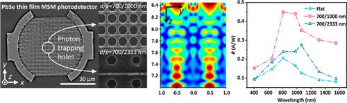
在表面集成光子捕获孔阵列的硅基硒化铅薄膜金属-半导体-金属(MSM)光电探测器在宽光谱范围内具有更高的效率。基于有限差分时域法,研究了薄膜厚度、衬底、孔结构(直径、周期和深度)和顶部电极对光电探测器红外吸收的影响,以优化器件结构。光子捕获孔阵列有效地减少了表面反射,并使垂直入射光在器件内形成横向慢速传播模式,从而增强了吸收。此外,还可以通过改变孔的周期来调整吸收峰值波长。我们制作了几种具有不同孔结构的硅基硒化铅薄膜 MSM 光电探测器,测得的效率与红外吸收的理论预测值非常吻合。在直径/周期比(d/p)为 700/1000 nm 的方形晶格中具有孔阵列的光电探测器在 808 nm 波长处的响应率为 0.449 A/W。与没有孔结构的器件相比,808、1064、1310 和 1550 纳米波长的响应率分别显著提高了 225%、267%、334% 和 357%。在 808 纳米波段和 1550 纳米波段的比检测率分别达到 1.474 × 10⁹ 琼斯和 9.3 × 10⁸ 琼斯。这项研究为在宽光谱范围内实现高效率的硅基单芯片集成光电二极管提供了一种新方法,这使得微孔支持的硅基 PbSe MSM 光电二极管有望覆盖 C、L 甚至更宽的波段,用于低成本红外传感和通信应用。
本文章由计算机程序翻译,如有差异,请以英文原文为准。

Enhanced Response of Si-Based PbSe Thin Film MSM Photodetectors by Photon-Trapping Hole Array in the Surface

Enhanced Response of Si-Based PbSe Thin Film MSM Photodetectors by Photon-Trapping Hole Array in the Surface
A Si-based PbSe thin film metal–semiconductor–metal (MSM) photodetector with enhanced efficiency in a wide spectral range is demonstrated with an integrated photon-trapping hole array in the surface. Based on the finite difference time domain method, the effects of film thickness, substrate, hole structure (diameter, period, and depth), and top electrodes on the infrared absorption of the photodetector are studied to optimize the device structure. The photon-trapping hole array effectively reduces the surface reflection and induces laterally slow propagating modes of the vertically incident light within the device, thereby achieving enhanced absorption. Additionally, the peak absorption wavelength can be tuned by changing the period of the holes. Several Si-based PbSe thin film MSM photodetectors with various hole structures are fabricated, and the measured efficiency agrees well with the theoretical prediction of infrared absorption. The photodetector with a hole array in a square lattice with a diameter/period ratio (d/p) of 700/1000 nm achieves a responsivity of 0.449 A/W at 808 nm. Compared to the device without hole structures, the responsivities at 808, 1064, 1310, and 1550 nm show significant enhancements of 225%, 267%, 334%, and 357%, respectively. The specific detectivity reaches 1.474 × 10⁹ Jones at 808 nm and 9.3 × 10⁸ Jones at 1550 nm. This study provides a new approach for the Si-based single-chip-integrated photodetectors with high efficiency over a broad spectral range, which makes the microhole-enabled Si-based PbSe MSM photodiodes promising to cover C, L, and even wider bands for low-cost infrared sensing and communication applications.
求助全文
通过发布文献求助,成功后即可免费获取论文全文。 去求助
来源期刊
ACS Photonics
ACS Photonics NANOSCIENCE & NANOTECHNOLOGY-MATERIALS SCIENCE, MULTIDISCIPLINARY
CiteScore
11.90
自引率
5.70%
发文量
438
审稿时长
2.3 months
期刊介绍: Published as soon as accepted and summarized in monthly issues, ACS Photonics will publish Research Articles, Letters, Perspectives, and Reviews, to encompass the full scope of published research in this field.
×
引用
GB/T 7714-2015
复制
MLA
复制
APA
复制
导出至
BibTeX EndNote RefMan NoteFirst NoteExpress
×
提示
您的信息不完整,为了账户安全,请先补充。
现在去补充
×
提示
您因"违规操作"
具体请查看互助需知
我知道了
×
提示
确定
请完成安全验证×
copy
已复制链接
快去分享给好友吧!
我知道了
右上角分享
点击右上角分享
0
联系我们:info@booksci.cn Book学术提供免费学术资源搜索服务,方便国内外学者检索中英文文献。致力于提供最便捷和优质的服务体验。 Copyright © 2023 布克学术 All rights reserved.
京ICP备2023020795号-1
ghs 京公网安备 11010802042870号
Book学术文献互助
Book学术文献互助群
群 号:604180095
Book学术官方微信